Article

Formamidinium Lead Iodide Perovskite Thin Films Formed by Two-Step Sequential Method: Solvent–Morphology Relationship

1
Institute of Macromolecular Chemistry, Czech Academy of Sciences, Heyrovského nám. 2, 162 00 Prague 6, Czech Republic
2
Department of Chemistry, Hanyang University, Seoul 04763, Republic of Korea
3
Institute of Nano Science and Technology, Hanyang University, Seoul 04763, Republic of Korea
4
Research Institute for Natural Sciences, Hanyang University, Seoul 04763, Republic of Korea
*
Author to whom correspondence should be addressed.
Materials 2023, 16(3), 1049; https://doi.org/10.3390/ma16031049
Submission received: 13 December 2022 / Revised: 11 January 2023 / Accepted: 19 January 2023 / Published: 25 January 2023
(This article belongs to the Special Issue Advances in Functional Materials and Nanodevices)

Abstract

:
Thin films made of formamidinium lead iodide (FAPbI3) perovskites prepared by a two-step sequential deposition method using various solvents for formamidinium iodide (FAI) - isopropanol, n-butanol and tert-butanol, were studied with the aim of finding a correlation between morphology and solvent properties to improve film quality. They were characterized by X-ray diffraction (XRD) and scanning electron microscopy (SEM) and their photophysical properties were studied by means of absorption and photoluminescence (PL) spectroscopies. XRD patterns, absorption and PL spectra proved α-phase formation for all selected solvents. An excessive amount of PbI2 found in perovskite films prepared with n-butanol indicates incomplete conversion. Thin film morphology, such as grain and crystallite size, depended on the solvent. Using tert-butanol, thin films with a very large grain size of up to several micrometers and with preferred crystallite orientation were fabricated. The grain size increased as follows: 0.2–0.5, 0.2–1 and 2–5 µm for isopropanol, n-butanol and tert-butanol, respectively. A correlation between the grain size and viscosity, electric permittivity and polarizability of the solvent could be considered. Our results, including fabrication of perovskite films with large grains and fewer grain boundaries, are important and of interest for many optoelectronic applications.

1. Introduction

Organic-inorganic perovskites have emerged as a highly promising class of semiconductor for optoelectronic device applications, such as solar cells [1,2,3,4,5,6,7], light-emitting diodes (LEDs) [8,9,10,11] and photodetectors [12,13,14,15] due to their many advantages including their low-cost, facile synthesis, solution processability, high absorption coefficient in the visible region, direct bandgap, ease of bandgap tuning and high luminescence quantum yield [16]. The power conversion efficiency (PCE) of perovskite solar cells was raised to 25.5% [7] and the external quantum efficiencies of LEDs based on perovskites exceeded 20% [11]. They have also shown potential in non-linear photonics [17] and as stimuli-responsive materials for a range of important technologies such as smart windows, memory devices, data storage and sensors [18,19,20,21]. Three-dimensional (3D) perovskite structures are formed by three primary ions ABX3 (A = Cs+, (CH3NH3)+ (MA), [HC(NH2)2]+ (FA); B = Pb2+, Ge2+, Sn2+; X = Cl, Br, I). The A and B cations coordinate with 12 and 6 X anions, respectively, forming cub-octahedral and octahedral structures. In general, stable 3D perovskite structures are formed when the tolerance factor is within the range of 0.76–1.13, while other perovskite-related structures are stable outside this range [22]. The prototype methylammonium lead iodide (MAPbI3) perovskite and the mixed halide MAPb(I1−xBrx)3 and MAPb(I1−xClx)3 analogues have dominated the field of organometallic halide perovskite materials. In addition to MA, FA was used to provide perovskite with a smaller bandgap (~1.5 eV). Formamidinium lead iodide (FAPbI3) perovskite shows great advantages in photovoltaic applications not only due to its ideal bandgap energy, but also due to better charge transport properties and better environmental stability, since the instability of MA-based perovskite is partly due to the hydrophilic nature of MA [23]. The difference in ionic radius of the MA (1.8 Å) and FA (1.9–2.2 Å) ions leads to structural and optoelectrical differences between MAPbI3 and FAPbI3. It was shown that MAPbI3 displays an n-type and FAPbI3 a p-type character [24,25]. The hole-diffusion length (~90 nm) in MAPbI3 is shorter than its electron-diffusion length (~130 nm) [26], while the hole-diffusion length in FAPbI3 (~813 nm) is 4.6 times larger than its electron-diffusion length (~177 nm) [27].
FAPbI3 has four main different crystal structures. The common crystal forms are perovskite α-FAPbI3 and non-perovskite δ-FAPbI3 phase. Distortions by the presence of [PbI6]4− octahedra promote the formation of lowered-symmetry β-FAPbI3 and γ-FAPbI3 black phases as the temperature decreases [28,29]. Pure α-FAPbI3 phase, as a very promising material for optoelectronic devices, is of great interest in the research field of perovskites. The performance of FAPbI3 devices can be considerably improved by stabilizing the α-FAPbI3 phase, eliminating lattice stress, improving the crystallinity and optimizing the device architecture [24,30]. Improvement of the film morphology of perovskite, i.e., fabrication of film with larger grains and fewer grain boundaries, is an important issue in optoelectronic applications, including photovoltaic devices.
One-step spin coating [31,32] and two-step sequential deposition [33,34,35,36,37,38,39] methods are commonly utilized for thin film preparation [40]. Anti-solvents are used to tune the nucleation and crystal/grain growth of perovskite precursor films in the one-step method. The film and conversion quality are influenced by anti-solvent delay dripping time. The anti-solvent treatment improves the surface morphology and promotes the crystal growth of perovskite films depending on their boiling point and polarity in relation to volatility and low solubility of perovskites compared to strong polar solvents [41]. Although the one-step method is very simple for thin film preparation, there is a problem with uneven surface coverage affecting the uniformity of the resulting film due to the uncontrollable rate of film crystallization. Various solvent and annealing engineering strategies have been developed to improve thin film quality and large grain formation [42,43,44,45,46,47]. The two-step sequential deposition of perovskite is an alternative route to one-step deposition, providing an efficient low-cost route to high performance perovskite films for optoelectronic applications. The advantage of the two-step method is easy fabrication of good-quality, pinhole-free thin films and better repeatability/reproducibility compared with the one-step method [48]. In this case, individual precursor layers are deposited separately and react with each other due to interdiffusion, forming thus a perovskite. In the sequential deposition, which was widely reported in MAPbI3 perovskite solar cells, two main routes were used. The first, in which a porous PbI2 is dipped in a MAI solution of isopropanol (IPA), leads to formation of the perovskite, where the dipping time is the critical parameter in the conversion of the perovskite phase, since interdiffusion is facilitated by the penetration of MAI into a porous PbI2 layer. In the second route, first PbI2 layer is prepared by spin coating a solution of PbI2 in N,N-dimethylformamide (DMF) and this is followed by spin coating a solution MAI in IPA on the top. The PbI2 layer has a very low solubility in IPA, therefore is not affected by the MAI spin coating. The interdiffusion method in stacked bilayers was described as different from the two-step dip coating method, as the interdiffusion reaction between precursor elements leading to perovskite is driven by thermal annealing at various temperatures for variable times, depending on the elements [40]. Recently, in-situ optical spectroscopy was used to study thin film formation of the model halide perovskite MAPbI3 during the spin coating of MAI on PbI2 in two-step coating and to understand the film formation dynamics [38]. It was found that the film formation takes place in five consecutive steps, including the initial formation of a MAPbI3 capping layer via an interface crystallization and the occurrence of an intense dissolution–recrystallization process leading to a fully converted temporally stable state.
In the two-step sequential method, IPA is commonly used as a solvent for the MAI (FAI). The solvents for inorganic (PbI2) and organic (MAI, FAI) components affect the quality and morphology of the perovskite film. There are more studies on solvent engineering concerning inorganic PbI2 than on organic components. As mentioned above, IPA is mostly used as solvent for organic components MAI or FAI. Cyclohexane, ethanol and cyclohexane or n-butanol mixed with IPA were also used as solvents for MAI or MABr [39]. n-butanol was used as co-solvent (2% in IPA) for preparation of MAPbI3 thin films possessing larger grain size (100–500 nm) for solar cells with improved PCE [49]. They attributed the improvement in the grain size to the slower solvent evaporation rate due to the addition of n-butanol with higher boiling point compared to IPA. Here, we have chosen IPA, n-butanol (n-BuOH) and tert-butanol (t-BuOH) as the solvents for FAI in perovskite fabrication, with the aim of revealing whether there is any correlation between the perovskite film morphology and solvent properties.
In this paper, we report on the preparation of organic-inorganic FAPbI3 perovskite thin films by a two-step sequential deposition method using various solvents (IPA, n-BuOH and t-BuOH) for FAI, on their characterization and on their photophysical properties. The structure and morphological properties of thin films were studied by X-ray diffraction (XRD) and scanning electron microscopy (SEM) and their photophysical properties by means of absorption and photoluminescence (PL) spectroscopies. Using t-BuOH, thin films with a very large grain size of up to several micrometers and preferred crystallite orientation were prepared. The obtained results are discussed in relation to the solvent properties used for FAI layer preparation. A correlation between grain size and solvent parameters is considered. To the best of our knowledge, the use of tert-butanol as a solvent for FAI in thin film preparation by the two-step sequential method producing FAPbI3 thin films with such large grains and such a correlation with the solvent properties have not been reported before.

2. Materials and Methods

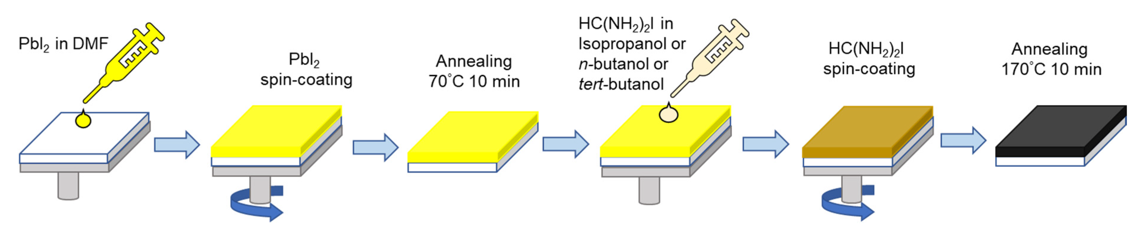
2.1. Materials and Layer Preparation

Formamidinium acetate, hydroiodic acid and solvents were purchased from commercial suppliers (TCI Europe, N.V., Zwijndrecht, Belgium, VWR International s.r.o., Stříbrná Skalice, Czech Republic, Lach-Ner, Ltd., Neratovice, Czech Republic).
Formamidinium iodide (FAI) was synthesized analogously to the literature [50,51,52,53] by the following procedure. Formamidinium acetate (TCI, 11.5 g, 0.11 mol) was dissolved in ethanol (80 mL) and the hydroiodic acid (57%, TCI, 30 mL, 0.227 mol HI) was slowly added. The reaction mixture was stirred at 50 °C for 2 h, then the solvents were vacuum evaporated and the residue was worked up with chloroform. The yellow crystals were filtered off, washed with chloroform (3 × 30 mL) and crystallized from ethanol/diethyl ether. Yield: 14.26 g of FAI (75%).
Lead iodide (PbI2) was prepared as follows. Lead nitrate (Pb(NO3)2, 2.42 g) dissolved in hot water (750 mL) and potassium iodide (KI, 2.42 g) dissolved in hot water (750 mL) were mixed in a 2L-Erlenmeyer flask and the mixture was heated (water bath) to obtain a clear solution. Then the flask was left for crystallization in a fridge overnight. The yellow precipitate of the PbI2 was filtered off (S2), washed with cold water to remove easily soluble KNO3 and dried (oil pump). Yield: 2.70 g (80%).
FAPbI3 thin film preparation was performed in the glove box (M. Braun Inertgas-Systeme GmbH, Garsching, Germany) under a nitrogen atmosphere in two steps by spin-coating. In the first step, the PbI2 dissolved in DMF (0.46 g mL−1, stirring at 70 °C overnight) was spin-coated at 3000 rpm for 30 s onto the fused silica substrates (UV-ozone for 15 min before the spin coating) and then annealed at 70 °C for 10 min. In the second step, the FAI (50 mg mL−1) dissolved in various solvents (IPA, n-BuOH and t-BuOH) was spin-coated at 1500–2500 rpm for 15 s on the top of the PbI2 layer and subsequently annealed at 170 °C for 10 min.

2.2. Methods

X-ray diffraction (XRD) measurements were performed in theta-2theta geometry from 2θ = 5°–45° with 0.01° step with Cu Kα radiation (1.54 Å) using an Explorer X-ray diffractometer (GNR Analytical Instruments, Novara, Italy). The beam was collimated using Soller slits and monochromatized by Ni filter and Mythen 1k Strip detector (CeleriX, Baden-Daettwil, Switzerland) with an active area of 62 mm × 8 mm and 1280 tailorable pixels. The sample−detector distance was 239.6 mm. A high-resolution FE-SEM (JEOL Ltd., Tokyo, Japan) JSM-7800F Prime (resolution: 0.7 nm at 15 kV) equipped with an in-lens Schottky plus field emission electron gun was used for the thin-film morphology characterization. A thin conductive layer of Pt with a thickness of ~20 Å was deposited on the films before SEM. Software VESTA was used for the structural model visualization [54]. UV–Vis spectra were measured on a Perkin-Elmer Lambda 35 UV/VIS spectrometer (PerkinElmer Instruments, Shelton, CT, USA). Photoluminescent (PL) spectra were recorded using a Perkin-Elmer LS55 Fluorescence spectrophotometer. Layer thicknesses (250–300 nm) were measured using a KLA-Tencor P-10 profilometer (KLA-Tencor Corporation, Milpitas, CA, USA). The measurements were performed at ambient atmosphere.

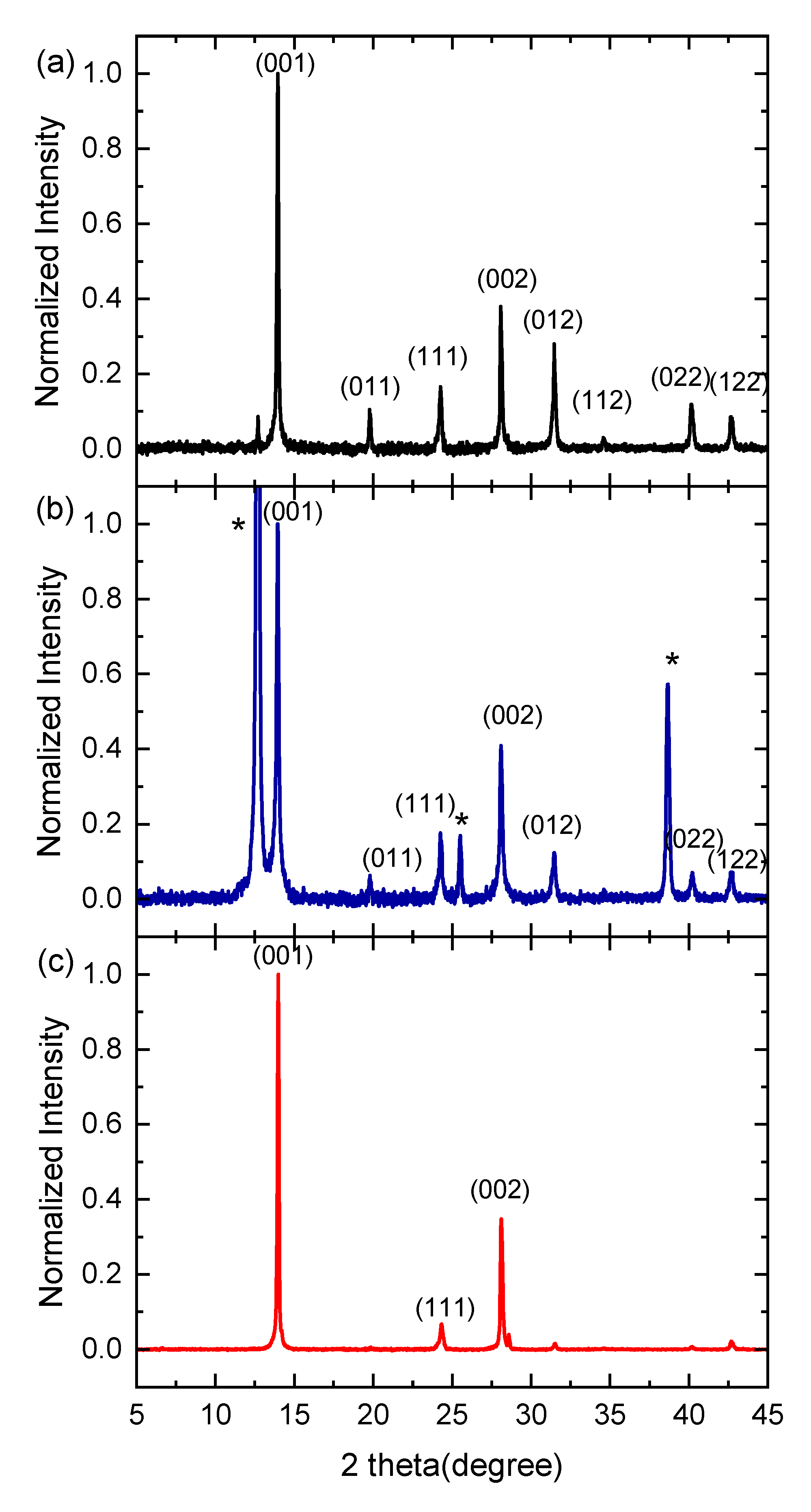
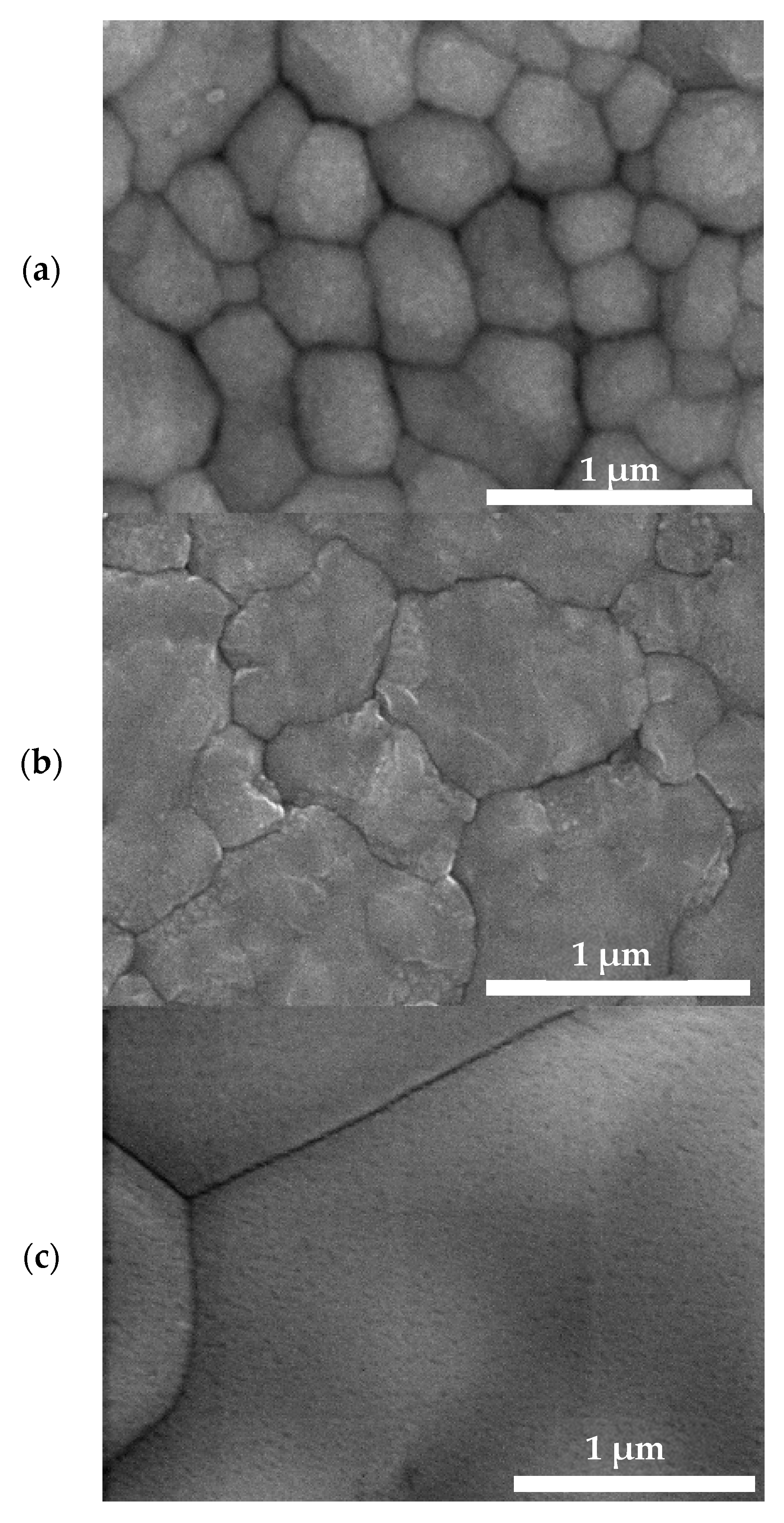
3. Results and Discussion

Thin FAPbI3 perovskite films were prepared by a two-step sequential deposition method, which is schematically shown in Figure 1. In the first step, the PbI2 layer was spin-coated from the DMF and in the second step FAI in various solvents (IPA, n-BuOH and t-BuOH) was used for the spin-coating process. After thin film annealing at 170 °C for 10 min, black FAPbI3 α-phase was obtained, which was confirmed by XRD measurements.
As already mentioned in the Introduction, the crystal structure of FAPbI3 is polymorphic due to the large ionic radius of FA. The structural diversity and phase behaviours of the FAPbI3 are related to the orientation of the FA cation and the degree of the crystal lattice distortion. In some of the literature, the α-FAPbI3 adopted a trigonal phase corresponding to P3m1 space group [25,55,56,57,58,59], but based on the crystal structure of α-FAPbI3 determined by high-resolution neutron powder diffraction, which is much more sensitive for the identification of light atom positions than XRD, it was shown to adopt a simpler cubic phase with Pm 3 ¯ m symmetry [60]. In the α-FAPbI3 crystal, the C–H in FA cation pointed directly toward the cube’s face and the FA cations with high rotational mobility are dynamically disordered within the octahedron framework due to the potential formation of hydrogen bonds between –NH2 and I [60,61]. A schematic view of the perovskite cubic structure and the structural model of FAPbI3 is shown in Figure 2.
X-ray patterns normalized to the dominant perovskite peak of FAPbI3 are displayed in Figure 3. The typical reflection peaks for FAPbI3 α-phase were identified for all films prepared using the selected solvents for FAI. XRD patterns of our films were verified as a single cubic phase, consistent with the literature [29,62,63,64,65,66,67,68]. XRD pattern of the films prepared with isopropanol shows peaks at 13.94°, 19.79°, 24.26°, 28.07°, 31.45°, 34.55°, 40.14° and 42.63° assigned to the reflections of the (001), (011), (111), (002), (012), (112), (022) and (122) crystal planes of cubic perovskite α-FAPbI3 structure, respectively. In the XRD pattern of FAPbI3 films prepared using n-BuOH as a solvent for FAI, the peaks at 12.7°, 25.5° and 38.7° appeared in addition to the perovskite peaks. These peaks (* in Figure 3b) with the dominating one at 12.7° correspond to PbI2 and indicate an incomplete perovskite conversion, related to the PbI2 excess. The PbI2 deposited from a DMF solution was crystallized as a hexagonal 2H polytype. The appearance of only three diffraction peaks corresponding to (001), (002) and (003) in XRD pattern lattice planes indicates the growth orientation along the c axis [40].
The XRD pattern for the FAPbI3 film prepared from t-BuOH exhibits two major (001) and (002) diffraction peaks at 13.97° and 28.1°, respectively. This observation indicated preferable growth along (001) and (002) crystallographic planes. In addition, a slight shift of the (001), (111) and (002) peaks to higher 2 θ values in the films compared with powder is likely due to the possible shrinking of the crystal lattice in the film. The lattice parameter values ( a ) given in Table 1 were evaluated using the Bragg relation n   λ = 2   d sin θ , where n is the order of the interference, λ is the X-ray wavelength, θ is the angle of incidence, d is the lattice plane spacing and the relation for the cubic crystal structure
1 d 2 = h 2 + k 2 + l 2 a 2
where h, k, l are the Miller indexes. Compared with the powder value of 0.6362 nm [60] the lower values in the range of 0.6342–0.6351 nm were obtained for all films, which correlate well with the average lattice parameter of 0.6335 nm obtained from the density functional theory (DFT) calculations [69].
Obvious differences in the ratios of peak intensity were found for the films prepared from different solvents, which indicates the influence of solvent on crystallinity and crystal orientation. The absolute intensity of both major peaks at 13.97° and 28.10° increased for the films prepared with t-BuOH, which shows the better crystallinity of these films than that of the films prepared with IPA or n-BuOH. A high degree of crystallinity is useful for optoelectronic applications because it facilitates charge carrier transport [59].
The XRD technique is a useful tool for determination of the crystallite size from the line broadening [70,71,72]. A primary source of peak broadening is related to the crystal domain size. The larger crystallites enhance intensity, while the smaller crystallites merge in the base of the peak. The relationship between peak full width at half maximum (FWHM) and the average crystallite size is given by the equation suggested by Scherrer in 1918 [73]
D = K λ β h k l cos θ
where λ is the X-ray wavelength, D the average crystallite size, β h k l the FWHM of the reflection peak located at angle 2 θ after subtraction of the instrumental broadening ( β h k l = β m e a s u r e d 2 β i n t r u m e n t a l 2 ), and K the Scherrer constant is a dimensionless shape factor. The value of K depends on the crystallite shape and the crystallite-size distribution and was found to be in the range of 0.62–2.08 [74]. There is uncertainty in K if the shape and distribution of crystallites are not known. The K value is typically at about 0.9. In our evaluation, we have used the value of 0.94, which is used for spherical crystallites with cubic crystal symmetry [70]. This method is applicable for the determination of the crystallite size of the order of 0.1 µm and appropriate for stress-free samples.
It should be noted that for thin films there are other sources of peak broadening that need to be considered. Thin-film materials are prone to maintain a certain strain in the lattice, which affects their average structure and shifts the peak positions (macrostrain); whereas the strain at a microscopic level (microstrain) affects the peak broadening [70]. There is strain induced in the sample due to crystal imperfection and distortion and distribution of strain within crystallites from the boundary to the core. We calculated the microstrain in the films by analysing the FWHM in the diffraction patterns according to the Williamson Hall (WH) plot method proposed by Williamson and Hall in 1953 [66]. This method is currently widely used for microstrain and crystallite size analysis for thin film polycrystalline samples to separate the crystallite size and strain contribution from XRD peak broadening. The relationship between the peak width β ε and microstrain ε is given by the Wilson equation [70]:
β ε = 4 ε tan θ
Combining Equations (1) and (2), the microstrain ε and crystallite size D in the films can be determined using the equation:
β h k l cos θ = K λ D + 4 ε sin θ
The slope and intercept of the straight line of the plot β h k l cos θ   vs .   sin θ give the value of microstrain and average crystallite size, respectively. The major peaks were used for evaluation. Very low microstrain values (<0.03%) were evaluated for all FAPbI3 films independent of the solvents used. The crystallite sizes are listed in Table 1. It was found that the solvent also influenced the crystallite size. The largest crystallite sizes are in the films prepared with t-BuOH and the smallest for the films prepared with n-BuOH, which possesses a higher boiling point and lower vapor pressure than the other two solvents.
The surface morphology was studied by SEM to compare the morphology of the thin films and to evaluate the size of grains in relation to the solvent used. Figure 4 shows SEM images of the FAPbI3 films. Larger grains were found in the films prepared using the n-BuOH and t-BuOH as a solvent for FAI than in the films where IPA was used (see Table 1). Very large grains of 2–5 µm were found in films prepared with t-BuOH. The advantage of large-size crystallites, grains and limitation of grain boundaries is that these usually lead to efficient charge carrier transport and hence to the improvement of optoelectronic devices. We tried to correlate the morphological data, grain and crystallite sizes with the properties of the solvents used for FAI spin-coating. Selected properties of the solvents, which were taken from the literature [75], are listed in Table 2. For the solvents under study, a correlation between the grain size and viscosity (µ), electric permittivity (εr) and polarizability (α) of the solvent could be considered. The grain size increased with increasing solvent viscosity and polarizability and with decreasing solvent electric permittivity. On the other hand, crystallite size could be considered in relation to the boiling point (Tbp) and vapor pressure(pv). Larger crystallite sizes were evaluated for the films prepared with IPA and t-BuOH, i.e., solvents having similar boiling point and vapor pressure, whereas the crystallite size was smaller for the films prepared using n-BuOH with a higher boiling point Tbp and lower vapor pressure pv.
Our findings could be correlated with description of the film formation as mentioned in the Introduction, reported for MAPbI3 film analyzed during preparation by two step spin-coating [38]. Analogously, the following steps can also be considered for the FAPbI3 film formation during FAI spin-coating on the top of PbI2 layer. In the first step, the FAPbI3 capping layer is formed on the top of PbI2, which prevents further FAPbI3 crystallization. Therefore, in the second step, the FAI solution concentration above the capping layer increases due to solvent evaporation. In the third step, the FAPbI3 capping layer begins to dissolve due to the increased iodine I- concentration as a result of progressing solvent evaporation. The fourth step involves a rapid main dissolution–recrystallization process, in which lead iodine complex Pb42− (formed by the reaction of PbI2 and 2I with the increasing concentration) reacts with FA cation leading to the FAPbI3 formation. The dissolution process of the capping layer generally occurs at the grain boundary and smaller grains, where new crystals are formed and increase the grain size. One can assume that the process is slower with increasing viscosity, which can facilitate larger grain formation. Finally, the complete fully converted and temporally stable state is formed in the fifth step.
Absorption and PL spectra have also confirmed FAPbI3 α-phase structure. Examples of absorption and PL spectra of the thin films are displayed in Figure 5 and photophysical data are summarized in Table 1.
The shapes of absorption spectra are typical for 3D black α-phase FAPbI3. Absorption coefficient values (in the range of 1.4–1.8 × 10⁷ m−1 at 500 nm, 6.6–7.5 × 10⁶ m−1 at 600 nm and 3.7–4.3 × 10⁶ m−1 at 700 nm) also correspond to those reported for this phase [69,76]. In the range of wavelength from 500 to 700 nm, the penetration depth values are from 55 to 270 nm. The bandgap (Eg) values evaluated from the Tauc plot (α*E)2 vs. E are about 1.5 eV, similar for all films prepared using IPA, n- and t-BuOH. They are in good agreement with the values reported for FAPbI3 thin films in the range of 1.46–1.53 eV [27,56,59,76,77] and are also consistent with the reported theoretical values from 1.44 to 1.6 eV [69,78,79]. PL peaks correspond well to the absorption onsets, which suggests that the observed photoluminescence is predominantly from the bandgap.

4. Conclusions

Morphology and photophysical properties of FAPbI3 thin films prepared by a two-step sequential deposition method using three different solvents for FAI (IPA, n-BuOH and t-BuOH) were studied. The morphology of thin films differed and was correlated with the selected solvent properties. A correlation between grain size and solvent viscosity, electric permeability and polarizability was found. We succeeded in the preparation of α-FAPbI3 thin films with large grains up to several micrometers with preferred crystallite orientation using t-BuOH as solvent for FAI. Grain size increased for the solvents as follows: IPA < n-BuOH < t-BuOH. This correlates with increasing solvent viscosity and polarizability and decreasing electric permittivity. In FAPbI3 films prepared using n-BuOH as a solvent for FAI, an excessive amount of PbI2 was found, which indicated an incomplete perovskite conversion. The evaluated crystallite sizes were largest for the FAPbI3 films prepared using t-BuOH, then with IPA, and the smallest sizes were evaluated for the films prepared with n-BuOH possessing higher boiling point and lower vapor pressure. The microstrain value was determined to be lower than 0.03% for all films under study. All FAPbI3 thin films exhibited a bandgap of about 1.5 eV and photoluminescence with maxima at 810–820 nm corresponding to the bandgap luminescence regardless of the solvent used for FAI. Our study provides insight into FAPbI3 thin film fabrication with large grains by two-step sequential deposition given by choice of solvent, which could be important for many optoelectronic applications.

Author Contributions

Conceptualization, V.C.; methodology, V.C. and Y.K.; formal analysis, V.C., M.G. and S.E.; investigation, V.C., M.G., S.E. and D.V.; resources, V.C., Y.K. and D.V.; writing—original draft preparation, V.C.; writing—review and editing, V.C., Y.K. and D.V.; visualization, V.C. and S.E.; supervision, V.C.; project administration, V.C.; funding acquisition, V.C. and Y.K. All authors have read and agreed to the published version of the manuscript.

Funding

This research was funded by Czech Science Foundation, grant number 20-15498J and National Research Foundation of Korea, grant number NRF-2019K2A9A1A06071525.

Institutional Review Board Statement

Not applicable.

Informed Consent Statement

Not applicable.

Data Availability Statement

Not applicable.

Acknowledgments

We thank the Czech Science Foundation and National Research Foundation of Korea for supporting this work under the framework of the international cooperation program with grants 20-15498J and NRF-2019K2A9A1A06071525, respectively.

Conflicts of Interest

The authors declare no conflict of interest.

References

  1. Jena, A.K.; Kulkarni, A.; Miyasaka, T. Halide Perovskite Photovoltaics: Background, Status, and Future Prospects. Chem. Rev. 2019, 119, 3036–3103. [Google Scholar] [CrossRef] [PubMed]
  2. Li, D.Y.; Zhang, D.Y.; Lim, K.S.; Hu, Y.; Rong, Y.G.; Mei, A.Y.; Park, N.G.; Han, H.W. A Review on Scaling Up Perovskite Solar Cells. Adv. Funct. Mater. 2021, 31, 2008621. [Google Scholar] [CrossRef]
  3. Zhang, X.W.; Shen, L.N.; Baral, P.; Vijayaraghavan, S.N.; Yan, F.; Gong, X.; Wang, H. Blade-coated inverted perovskite solar cells in an ambient environment. Sol. Energy Mater. Sol. Cells 2022, 246, 111894. [Google Scholar] [CrossRef]
  4. Yan, J.; Savenije, T.J.; Mazzarella, L.; Isabella, O. Progress and challenges on scaling up of perovskite solar cell technology. Sustain. Energy Fuels 2022, 6, 243–266. [Google Scholar] [CrossRef]
  5. Roy, P.; Ghosh, A.; Barclay, F.; Khare, A.; Cuce, E. Perovskite Solar Cells: A Review of the Recent Advances. Coatings 2022, 12, 1089. [Google Scholar] [CrossRef]
  6. Guo, Z.; Jena, A.K.; Kim, G.M.; Miyasaka, T. The high open-circuit voltage of perovskite solar cells: A review. Energy Environ. Sci. 2022, 15, 3171–3222. [Google Scholar] [CrossRef]
  7. Zhang, H.; Ji, X.; Yao, H.; Fan, Q.; Yu, B.; Li, J. Review on efficiency improvement effort of perovskite solar cell. Sol. Energy 2022, 233, 421–434. [Google Scholar] [CrossRef]
  8. Zhao, X.F.; Ng, J.D.A.; Friend, R.H.; Tan, Z.K. Opportunities and Challenges in Perovskite Light-Emitting Devices. Acs Photonics 2018, 5, 3866–3875. [Google Scholar] [CrossRef]
  9. Hassan, Y.; Park, J.H.; Crawford, M.L.; Sadhanala, A.; Lee, J.; Sadighian, J.C.; Mosconi, E.; Shivanna, R.; Radicchi, E.; Jeong, M.; et al. Ligand-engineered bandgap stability in mixed-halide perovskite LEDs. Nature 2021, 591, 72–77. [Google Scholar] [CrossRef]
  10. Kim, Y.-H.; Kim, S.; Kakekhani, A.; Park, J.; Park, J.; Lee, Y.-H.; Xu, H.; Nagane, S.; Wexler, R.B.; Kim, D.-H.; et al. Comprehensive defect suppression in perovskite nanocrystals for high-efficiency light-emitting diodes. Nat. Photonics 2021, 15, 148–155. [Google Scholar] [CrossRef]
  11. Yang, D.; Zhao, B.; Yang, T.; Lai, R.; Lan, D.; Friend, R.H.; Di, D. Toward Stable and Efficient Perovskite Light-Emitting Diodes. Adv. Funct. Mater. 2022, 32, 2109495. [Google Scholar] [CrossRef]
  12. Miao, J.L.; Zhang, F.J. Recent progress on highly sensitive perovskite photodetectors. J. Mater. Chem. C 2019, 7, 1741–1791. [Google Scholar] [CrossRef]
  13. Zhou, J.; Huang, J. Photodetectors Based on Organic-Inorganic Hybrid Lead Halide Perovskites. Adv. Sci. 2018, 5, 1700256. [Google Scholar] [CrossRef]
  14. Wang, T.; Lian, G.; Huang, L.; Zhu, F.; Cui, D.; Wang, Q.; Meng, Q.; Jiang, H.; Zhou, G.; Wong, C.-P. A crystal-growth boundary-fusion strategy to prepare high-quality MAPbI3 films for excellent Vis-NIR photodetectors. Nano Energy 2019, 64, 103914. [Google Scholar] [CrossRef]
  15. Wang, T.; Zheng, D.M.; Zhang, J.K.; Qiao, J.; Min, C.J.; Yuan, X.C.; Somekh, M.; Feng, F. High-Performance and Stable Plasmonic-Functionalized Formamidinium-Based Quasi-2D Perovskite Photodetector for Potential Application in Optical Communication. Adv. Funct. Mater. 2022, 32, 2208694. [Google Scholar] [CrossRef]
  16. Kim, J.Y.; Lee, J.W.; Jung, H.S.; Shin, H.; Park, N.G. High-Efficiency Perovskite Solar Cells. Chem. Rev. 2020, 120, 7867–7918. [Google Scholar] [CrossRef]
  17. Chen, W.; Zhang, F.; Wang, C.; Jia, M.; Zhao, X.; Liu, Z.; Ge, Y.; Zhang, Y.; Zhang, H. Nonlinear Photonics Using Low-Dimensional Metal-Halide Perovskites: Recent Advances and Future Challenges. Adv. Mater. 2021, 33, e2004446. [Google Scholar] [CrossRef]
  18. Zhumekenov, A.A.; Saidaminov, M.I.; Mohammed, O.F.; Bakr, O.M. Stimuli-responsive switchable halide perovskites: Taking advantage of instability. Joule 2021, 5, 2027–2046. [Google Scholar] [CrossRef]
  19. Syrrokostas, G.; Dokouzis, A.; Yannopoulos, S.N.; Leftheriotis, G. Novel photoelectrochromic devices incorporating carbon-based perovskite solar cells. Nano Energy 2020, 77, 105243. [Google Scholar] [CrossRef]
  20. Jiang, F.; Lee, P.S. Performance optimization strategies of halide perovskite-based mechanical energy harvesters. Nanoscale Horiz. 2022, 7, 1029–1046. [Google Scholar] [CrossRef]
  21. Minh, D.N.; Nguyen, L.A.T.; Trinh, C.T.; Oh, C.; Eom, S.; Vu, T.V.; Choi, J.; Sim, J.H.; Lee, K.-G.; Kim, J.; et al. Low-Dimensional Single-Cation Formamidinium Lead Halide Perovskites (FAm+2PbmBr3m+2): From Synthesis to Rewritable Phase-Change Memory Film. Adv. Funct. Mater. 2021, 31, 2011093. [Google Scholar] [CrossRef]
  22. Shamsi, J.; Urban, A.S.; Imran, M.; De Trizio, L.; Manna, L. Metal Halide Perovskite Nanocrystals: Synthesis, Post-Synthesis Modifications, and Their Optical Properties. Chem. Rev. 2019, 119, 3296–3348. [Google Scholar] [CrossRef] [PubMed]
  23. Hu, S.; Xiang, C.H.; Yan, P.Y.; Zhang, Y.; Li, H.; Sheng, C.X. Highly efficient inverted planar solar cell using formamidinium-based quasi-two dimensional perovskites. J. Alloy. Compd. 2022, 921, 166139. [Google Scholar] [CrossRef]
  24. Jeon, N.J.; Noh, J.H.; Yang, W.S.; Kim, Y.C.; Ryu, S.; Seo, J.; Seok, S.I. Compositional engineering of perovskite materials for high-performance solar cells. Nature 2015, 517, 476–480. [Google Scholar] [CrossRef]
  25. Stoumpos, C.C.; Malliakas, C.D.; Kanatzidis, M.G. Semiconducting tin and lead iodide perovskites with organic cations: Phase transitions, high mobilities, and near-infrared photoluminescent properties. Inorg. Chem. 2013, 52, 9019–9038. [Google Scholar] [CrossRef]
  26. Xing, G.; Mathews, N.; Sun, S.; Lim, S.S.; Lam, Y.M.; Gratzel, M.; Mhaisalkar, S.; Sum, T.C. Long-range balanced electron- and hole-transport lengths in organic-inorganic CH3NH3PbI3. Science 2013, 342, 344–347. [Google Scholar] [CrossRef]
  27. Eperon, G.E.; Stranks, S.D.; Menelaou, C.; Johnston, M.B.; Herz, L.M.; Snaith, H.J. Formamidinium lead trihalide: A broadly tunable perovskite for efficient planar heterojunction solar cells. Energy Environ. Sci. 2014, 7, 982–988. [Google Scholar] [CrossRef]
  28. Masi, S.; Gualdrón-Reyes, A.F.; Mora-Seró, I. Stabilization of Black Perovskite Phase in FAPbI3 and CsPbI3. Acs Energy Lett. 2020, 5, 1974–1985. [Google Scholar] [CrossRef]
  29. Fabini, D.H.; Stoumpos, C.C.; Laurita, G.; Kaltzoglou, A.; Kontos, A.G.; Falaras, P.; Kanatzidis, M.G.; Seshadri, R. Reentrant Structural and Optical Properties and Large Positive Thermal Expansion in Perovskite Formamidinium Lead Iodide. Angew. Chem. Int. Ed. 2016, 55, 15392–15396. [Google Scholar] [CrossRef] [Green Version]
  30. Zheng, Z.; Wang, S.; Hu, Y.; Rong, Y.; Mei, A.; Han, H. Development of formamidinium lead iodide-based perovskite solar cells: Efficiency and stability. Chem. Sci. 2022, 13, 2167–2183. [Google Scholar] [CrossRef]
  31. Sajid, S.; Khan, S.; Khan, A.; Khan, D.; Issakhov, A.; Park, J. Antisolvent-fumigated grain growth of active layer for efficient perovskite solar cells. Sol. Energy 2021, 225, 1001–1008. [Google Scholar] [CrossRef]
  32. Chen, S.; Xiao, X.; Chen, B.; Kelly, L.L.; Zhao, J.; Lin, Y.; Toney, M.F.; Huang, J. Crystallization in one-step solution deposition of perovskite films: Upward or downward? Sci. Adv. 2021, 7, eabb2412. [Google Scholar] [CrossRef]
  33. Burschka, J.; Pellet, N.; Moon, S.-J.; Humphry-Baker, R.; Gao, P.; Nazeeruddin, M.K.; Grätzel, M. Sequential deposition as a route to high-performance perovskite-sensitized solar cells. Nature 2013, 499, 316–319. [Google Scholar] [CrossRef]
  34. Hu, L.; Peng, J.; Wang, W.W.; Xia, Z.; Yuan, J.Y.; Lu, J.L.; Huang, X.D.; Ma, W.L.; Song, H.B.; Chen, W.; et al. Sequential Deposition of CH3NH3PbI3 on Planar NiO Film for Efficient Planar Perovskite Solar Cells. ACS Photonics 2014, 1, 547–553. [Google Scholar] [CrossRef]
  35. Xiao, Z.G.; Bi, C.; Shao, Y.C.; Dong, Q.F.; Wang, Q.; Yuan, Y.B.; Wang, C.G.; Gao, Y.L.; Huang, J.S. Efficient, high yield perovskite photovoltaic devices grown by interdiffusion of solution-processed precursor stacking layers. Energy Environ. Sci. 2014, 7, 2619–2623. [Google Scholar] [CrossRef]
  36. Lee, J.W.; Park, N.G. Two-step deposition method for high-efficiency perovskite solar cells. MRS Bull. 2015, 40, 654–659. [Google Scholar] [CrossRef]
  37. Sajid, S.; Alzahmi, S.; Salem, I.B.; Obaidat, I.M. Perovskite-Surface-Confined Grain Growth for High-Performance Perovskite Solar Cells. Nanomaterials 2022, 12, 3352. [Google Scholar] [CrossRef]
  38. Chauhan, M.; Zhong, Y.; Schötz, K.; Tripathi, B.; Köhler, A.; Huettner, S.; Panzer, F. Investigating two-step MAPbI3 thin film formation during spin coating by simultaneous in situ absorption and photoluminescence spectroscopy. J. Mater. Chem. A 2020, 8, 5086–5094. [Google Scholar] [CrossRef]
  39. Han, Y.P.; Xie, H.B.; Lim, E.L.; Bi, D.Q. Review of Two-Step Method for Lead Halide Perovskite Solar Cells. Sol. RRL 2022, 6, 2101007. [Google Scholar] [CrossRef]
  40. Dubey, A.; Adhikari, N.; Mabrouk, S.; Wu, F.; Chen, K.; Yang, S.F.; Qiao, Q.Q. A strategic review on processing routes towards highly efficient perovskite solar cells. J. Mater. Chem. A 2018, 6, 2406–2431. [Google Scholar] [CrossRef]
  41. Jung, M.; Ji, S.-G.; Kim, G.; Seok, S.I. Perovskite precursor solution chemistry: From fundamentals to photovoltaic applications. Chem. Soc. Rev. 2019, 48, 2011–2038. [Google Scholar] [CrossRef] [PubMed]
  42. Taylor, A.D.; Sun, Q.; Goetz, K.P.; An, Q.; Schramm, T.; Hofstetter, Y.; Litterst, M.; Paulus, F.; Vaynzof, Y. A general approach to high-efficiency perovskite solar cells by any antisolvent. Nat. Commun. 2021, 12, 1878. [Google Scholar] [CrossRef] [PubMed]
  43. Fu, X.; Dong, N.; Lian, G.; Lv, S.; Zhao, T.; Wang, Q.; Cui, D.; Wong, C.P. High-Quality CH(3)NH(3)PbI(3) Films Obtained via a Pressure-Assisted Space-Confined Solvent-Engineering Strategy for Ultrasensitive Photodetectors. Nano Lett. 2018, 18, 1213–1220. [Google Scholar] [CrossRef] [PubMed]
  44. Rong, Y.; Tang, Z.; Zhao, Y.; Zhong, X.; Venkatesan, S.; Graham, H.; Patton, M.; Jing, Y.; Guloy, A.M.; Yao, Y. Solvent engineering towards controlled grain growth in perovskite planar heterojunction solar cells. Nanoscale 2015, 7, 10595–10599. [Google Scholar] [CrossRef] [PubMed]
  45. Ghosh, S.; Mishra, S.; Singh, T. Antisolvents in Perovskite Solar Cells: Importance, Issues, and Alternatives. Adv. Mater. Interfaces 2020, 7, 2000950. [Google Scholar] [CrossRef]
  46. Liu, R.Z.; Xu, K. Solvent engineering for perovskite solar cells: A review. Micro Nano Lett. 2020, 15, 349–353. [Google Scholar] [CrossRef]
  47. Wang, L.; Liu, G.L.; Xi, X.; Yang, G.F.; Hu, L.F.; Zhu, B.J.; He, Y.F.; Liu, Y.S.; Qian, H.Q.; Zhang, S.D.; et al. Annealing Engineering in the Growth of Perovskite Grains. Crystals 2022, 12, 894. [Google Scholar] [CrossRef]
  48. Wang, M.H.; Feng, Y.L.; Bian, J.M.; Liu, H.Z.; Shi, Y.T. A comparative study of one-step and two-step approaches for MAPbI(3) perovskite layer and its influence on the performance of mesoscopic perovskite solar cell. Chem. Phys. Lett. 2018, 692, 44–49. [Google Scholar] [CrossRef]
  49. Mou, J.P.; Song, J.; Che, M.; Liu, Y.; Qin, Y.S.; Liu, H.M.; Zhu, L.; Zhao, Y.L.; Qiang, Y.H. Butanol-assisted solvent annealing of CH3NH3PbI3 film for high-efficient perovskite solar cells. J. Mater. Sci. Mater. Electron. 2019, 30, 746–752. [Google Scholar] [CrossRef]
  50. Wang, F.; Yu, H.; Xu, H.H.; Zhao, N. HPbI3: A New Precursor Compound for Highly Efficient Solution-Processed Perovskite Solar Cells. Adv. Funct. Mater. 2015, 25, 1120–1126. [Google Scholar] [CrossRef]
  51. Bag, M.; Renna, L.A.; Adhikari, R.Y.; Karak, S.; Liu, F.; Lahti, P.M.; Russell, T.P.; Tuominen, M.T.; Venkataraman, D. Kinetics of Ion Transport in Perovskite Active Layers and Its Implications for Active Layer Stability. J. Am. Chem. Soc. 2015, 137, 13130–13137. [Google Scholar] [CrossRef]
  52. Weber, O.J.; Charles, B.; Weller, M.T. Phase behaviour and composition in the formamidinium-methylammonium hybrid lead iodide perovskite solid solution. J. Mater. Chem. A 2016, 4, 15375–15382. [Google Scholar] [CrossRef] [Green Version]
  53. Yang, W.S.; Park, B.W.; Jung, E.H.; Jeon, N.J.; Kim, Y.C.; Lee, D.U.; Shin, S.S.; Seo, J.; Kim, E.K.; Noh, J.H.; et al. Iodide management in formamidinium-lead-halide-based perovskite layers for efficient solar cells. Science 2017, 356, 1376–1379. [Google Scholar] [CrossRef] [Green Version]
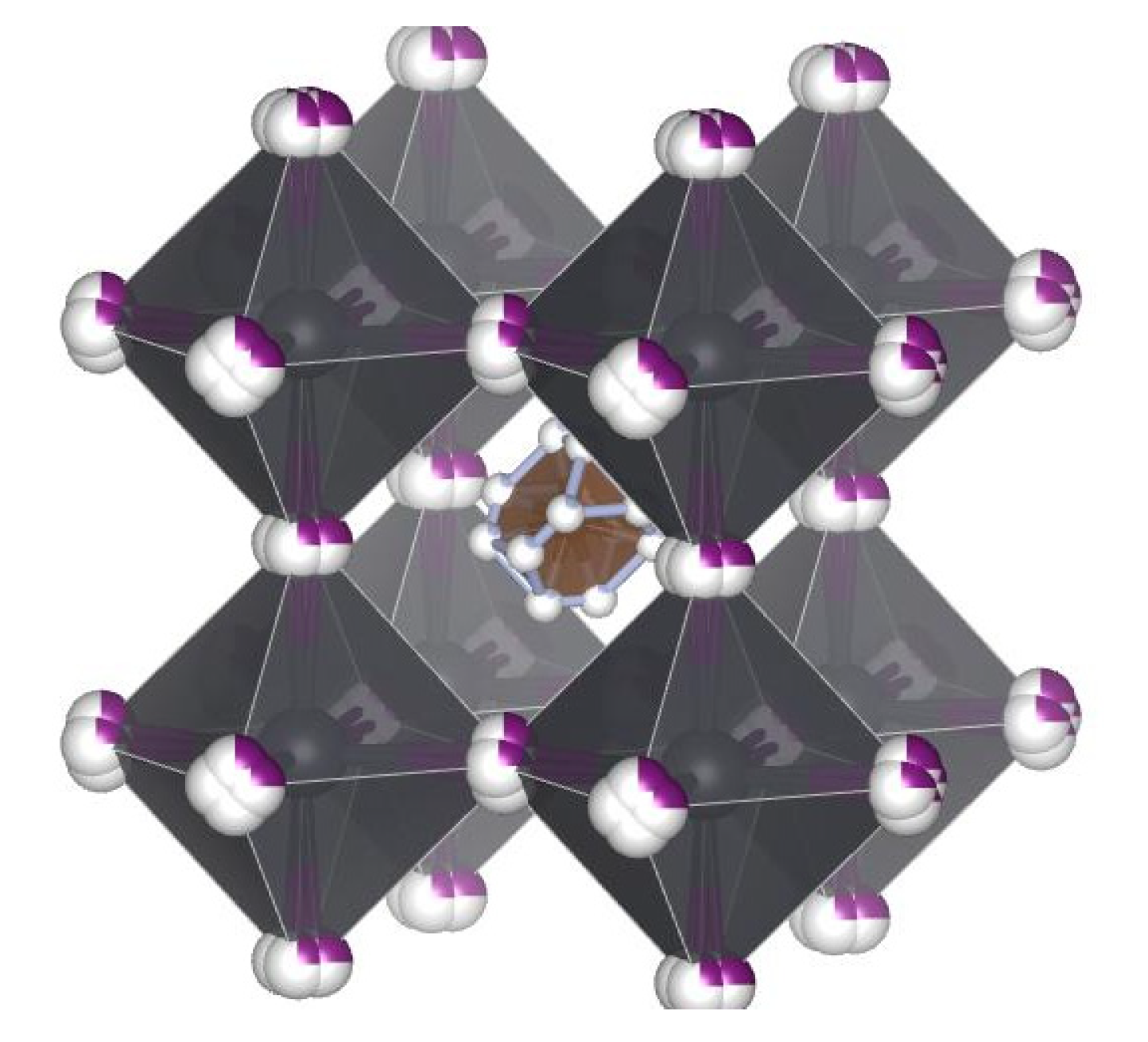
  54. Momma, K.; Izumi, F. VESTA 3 for three-dimensional visualization of crystal, volumetric and morphology data. J. Appl. Cryst. 2011, 44, 1272–1276. [Google Scholar] [CrossRef]
  55. Koh, T.M.; Fu, K.W.; Fang, Y.N.; Chen, S.; Sum, T.C.; Mathews, N.; Mhaisalkar, S.G.; Boix, P.P.; Baikie, T. Formamidinium-Containing Metal-Halide: An Alternative Material for Near-IR Absorption Perovskite Solar Cells. J. Phys. Chem. C 2014, 118, 16458–16462. [Google Scholar] [CrossRef]
  56. Binek, A.; Hanusch, F.C.; Docampo, P.; Bein, T. Stabilization of the Trigonal High-Temperature Phase of Formamidinium Lead Iodide. J. Phys. Chem. Lett. 2015, 6, 1249–1253. [Google Scholar] [CrossRef]
  57. Han, Q.; Bae, S.H.; Sun, P.; Hsieh, Y.T.; Yang, Y.M.; Rim, Y.S.; Zhao, H.; Chen, Q.; Shi, W.; Li, G.; et al. Single Crystal Formamidinium Lead Iodide (FAPbI3): Insight into the Structural, Optical, and Electrical Properties. Adv. Mater. 2016, 28, 2253–2258. [Google Scholar] [CrossRef]
  58. Yang, S.D.; Liu, W.Q.; Zuo, L.J.; Zhang, X.Q.; Ye, T.; Chen, J.H.; Li, C.Z.; Wu, G.; Chen, H.Z. Thiocyanate assisted performance enhancement of formamidinium based planar perovskite solar cells through a single one-step solution process. J. Mater. Chem. A 2016, 4, 9430–9436. [Google Scholar] [CrossRef]
  59. Zhang, M.; Zhang, F.; Wang, Y.; Zhu, L.; Hu, Y.; Lou, Z.; Hou, Y.; Teng, F. High-Performance Photodiode-Type Photodetectors Based on Polycrystalline Formamidinium Lead Iodide Perovskite Thin Films. Sci. Rep. 2018, 8, 11157. [Google Scholar] [CrossRef] [Green Version]
  60. Weller, M.T.; Weber, O.J.; Frost, J.M.; Walsh, A. Cubic Perovskite Structure of Black Formamidinium Lead Iodide, α-[HC(NH2)2]PbI3, at 298 K. J. Phys. Chem. Lett. 2015, 6, 3209–3212. [Google Scholar] [CrossRef]
  61. Chen, H.; Chen, Y.; Zhang, T.; Liu, X.; Wang, X.; Zhao, Y. Advances to High-Performance Black-Phase FAPbI3 Perovskite for Efficient and Stable Photovoltaics. Small Struct. 2021, 2, 2000130. [Google Scholar] [CrossRef]
  62. Saidaminov, M.I.; Abdelhady, A.L.; Maculan, G.; Bakr, O.M. Retrograde solubility of formamidinium and methylammonium lead halide perovskites enabling rapid single crystal growth. Chem. Commun. 2015, 51, 17658–17661. [Google Scholar] [CrossRef] [Green Version]
  63. Zhumekenov, A.A.; Saidaminov, M.I.; Haque, M.A.; Alarousu, E.; Sarmah, S.P.; Murali, B.; Dursun, I.; Miao, X.H.; Abdelhady, A.L.; Wu, T.; et al. Formamidinium Lead Halide Perovskite Crystals with Unprecedented Long Carrier Dynamics and Diffusion Length. ACS Energy Lett. 2016, 1, 32–37. [Google Scholar] [CrossRef]
  64. Liu, Y.C.; Sun, J.K.; Yang, Z.; Yang, D.; Ren, X.D.; Xu, H.; Yang, Z.P.; Liu, S.Z. 20-mm-Large Single-Crystalline Formamidinium-Perovskite Wafer for Mass Production of Integrated Photodetectors. Adv. Opt. Mater. 2016, 4, 1829–1837. [Google Scholar] [CrossRef]
  65. Sekimoto, T.; Suzuka, M.; Yokoyama, T.; Uchida, R.; Machida, S.; Sekiguchi, T.; Kawano, K. Energy level diagram of HC(NH(2))(2)PbI(3) single crystal evaluated by electrical and optical analyses. Phys. Chem. Chem. Phys. 2018, 20, 1373–1380. [Google Scholar] [CrossRef]
  66. Murugadoss, G.; Thangamuthu, R.; Kumar, M.R. Formamidinium lead iodide perovskite: Structure, shape and optical tuning via hydrothermal method. Mater. Lett. 2018, 231, 16–19. [Google Scholar] [CrossRef]
  67. Murugadoss, G.; Kuppusami, P.; Kumar, M.R. Solvent effect on structure and morphology of formamidinium lead tri-iodide perovskite via hydrothermal method. Inorg. Chem. Commun. 2020, 119, 108059. [Google Scholar] [CrossRef]
  68. Murugadoss, G.; Arunachalam, P.; Panda, S.K.; Rajesh Kumar, M.; Rajabathar, J.R.; Al-Lohedan, H.; Wasmiah, M.D. Crystal stabilization of α-FAPbI3 perovskite by rapid annealing method in industrial scale. J. Mater. Res. Technol. 2021, 12, 1924–1930. [Google Scholar] [CrossRef]
  69. Kato, M.; Fujiseki, T.; Miyadera, T.; Sugita, T.; Fujimoto, S.; Tamakoshi, M.; Chikamatsu, M.; Fujiwara, H. Universal rules for visible-light absorption in hybrid perovskite materials. J. Appl. Phys. 2017, 121, 115501. [Google Scholar] [CrossRef] [Green Version]
  70. Harrington, G.F.; Santiso, J. Back-to-Basics tutorial: X-ray diffraction of thin films. J. Electroceram. 2021, 47, 141–163. [Google Scholar] [CrossRef]
  71. Pandey, A.; Dalal, S.; Dutta, S.; Dixit, A. Structural characterization of polycrystalline thin films by X-ray diffraction techniques. J. Mater. Sci. Mater. Electron. 2021, 32, 1341–1368. [Google Scholar] [CrossRef]
  72. Hossain, M.K.; Yamamoto, T.; Hashizume, K. Effect of sintering conditions on structural and morphological properties of Y- and Co-doped BaZrO3 proton conductors. Ceram. Int. 2021, 47, 27177–27187. [Google Scholar] [CrossRef]
  73. Scherrer, P. Bestimmung der Größe und der inneren Struktur von Kolloidteilchen mittels Röntgenstrahlen. Nachr. Ges. Wiss. Göttingen Math. Phys. Kl. 1918, 2, 98–100. [Google Scholar]
  74. Langford, J.I.; Wilson, A.J.C. Scherrer after sixty years: A survey and some new results in the determination of crystallite size. J. Appl. Cryst. 1978, 11, 102–113. [Google Scholar] [CrossRef]
  75. Bosque, R.; Sales, J. Polarizabilities of Solvents from the Chemical Composition. J. Chem. Inf. Comput. Sci. 2002, 42, 1154–1163. [Google Scholar] [CrossRef]
  76. Lee, J.W.; Seol, D.J.; Cho, A.N.; Park, N.G. High-efficiency perovskite solar cells based on the black polymorph of HC(NH2)2 PbI3. Adv. Mater. 2014, 26, 4991–4998. [Google Scholar] [CrossRef]
  77. Aharon, S.; Dymshits, A.; Rotem, A.; Etgar, L. Temperature dependence of hole conductor free formamidinium lead iodide perovskite based solar cells. J. Mater. Chem. A 2015, 3, 9171–9178. [Google Scholar] [CrossRef]
  78. El-Ghtami, H.; Laref, A.; Laref, S. Electronic and optical behaviors of methylammonium and formamidinium lead trihalide perovskite materials. J. Mater. Sci. Mater. Electron. 2019, 30, 711–720. [Google Scholar] [CrossRef]
  79. Pachori, S.; Kumari, S.; Verma, A.S. An emerging high performance photovoltaic device with mechanical stability constants of hybrid (HC(NH2)2PbI3) perovskite. J. Mater. Sci. Mater. Electron. 2020, 31, 18004–18017. [Google Scholar]
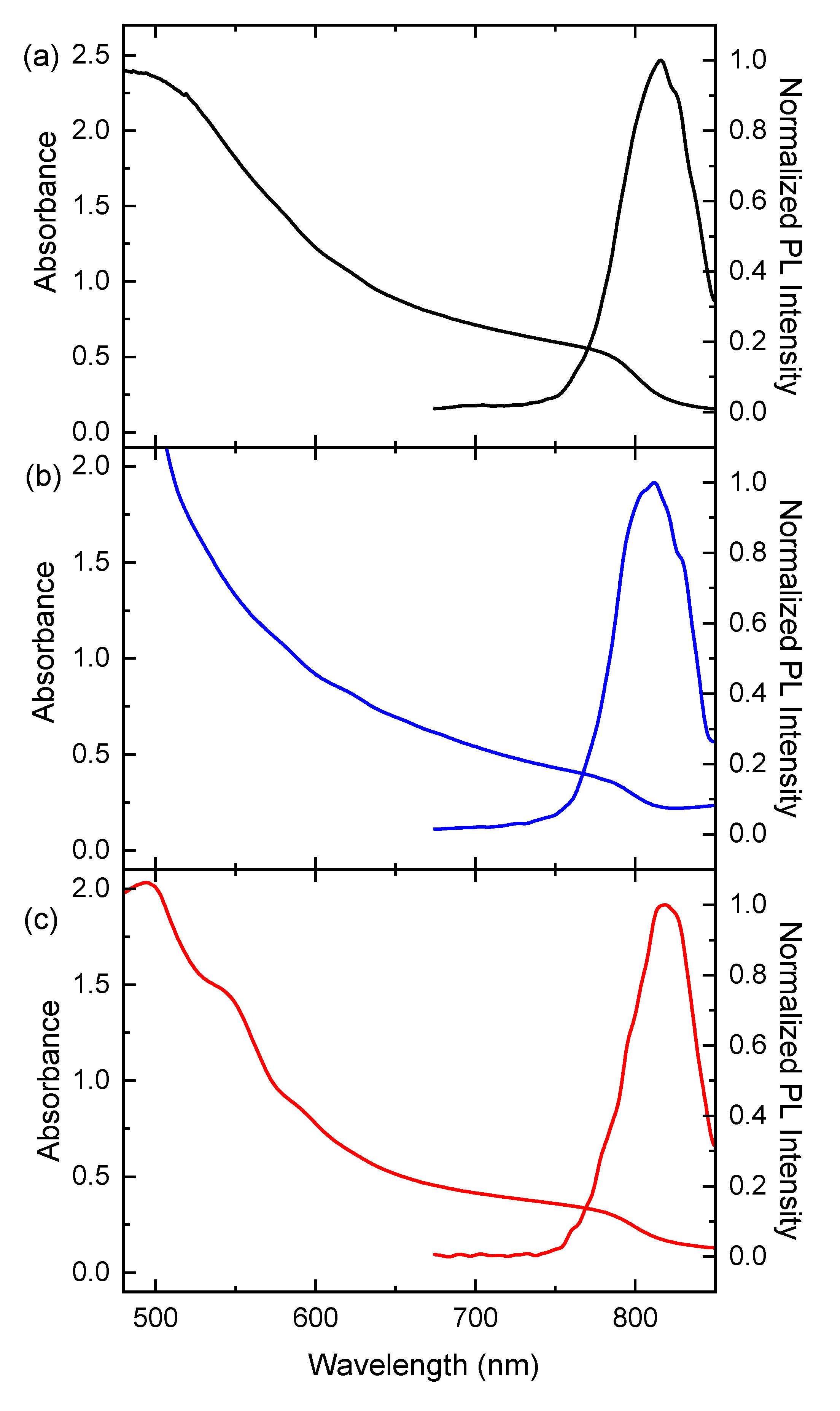
Figure 1. Scheme of two-step sequential deposition method of FAPbI3.
Materials 16 01049 g001
Figure 2. Schematic view of perovskite cubic structure and structural model of FAPbI3 (FA cation located in the middle).
Materials 16 01049 g002
Figure 3. Normalized X-ray (XRD) patterns of the thin film perovskite FAPbI3 prepared on fused silica by two-step method using various solvents for FAI: (a) IPA, (b) n-BuOH and (c) t-BuOH (* correspond to PbI2).
Materials 16 01049 g003
Figure 4. SEM images of the thin film perovskite FAPbI3 prepared by two-step method using various solvents for FAI: (a) IPA, (b) n-BuOH and (c) t-BuOH.
Materials 16 01049 g004
Figure 5. Absorption and PL spectra of the thin film perovskite FAPbI3 prepared by a two-step sequential deposition method using various solvents for FAI: (a) IPA, (b) n-BuOH and (c) t-BuOH.
Materials 16 01049 g005
Table 1. Morphological and photophysical data (a is lattice parameter, D crystallite size, L grain size, Eg bandgap, λPLmax maximum of photoluminescence).
Solventa (nm)D (nm)L (µm)Eg (eV)λPLmax (nm)
IPA0.635166–800.2–0.51.510816
n-BuOH0.634655–650.2–11.504812
t-BuOH0.634293–992–51.503818
Table 2. Selected properties of the solvents used for FAI (Mw—molar mass, ρ—density, Tbp—boiling point, ρv—vapor density, pv—vapor pressure, µ—viscosity, RP—relative polarity, εr—electric permittivity, µd—dipole moment, α—polarizability).
SolventMwρ (g/mL) at 25 °CTbp (°C)ρv (vs. Air)pv (hPa) at 20 °Cµ (10−3 Pa s)RPεrµd (D)α3)
IPA60.10.78582.42.1442.070.546191.666.98
n-BuOH74.120.81117.62.556.32.590.58617.51.78.79
t-BuOH74.120.77582.22.55413.350.38912.41.78.82
Disclaimer/Publisher’s Note: The statements, opinions and data contained in all publications are solely those of the individual author(s) and contributor(s) and not of MDPI and/or the editor(s). MDPI and/or the editor(s) disclaim responsibility for any injury to people or property resulting from any ideas, methods, instructions or products referred to in the content.

