
Effect of Europium Addition on the Microstructure and Dielectric Properties of CCTO Ceramic Prepared Using Conventional and Microwave Sintering

Abstract
:1. Introduction
2. Results
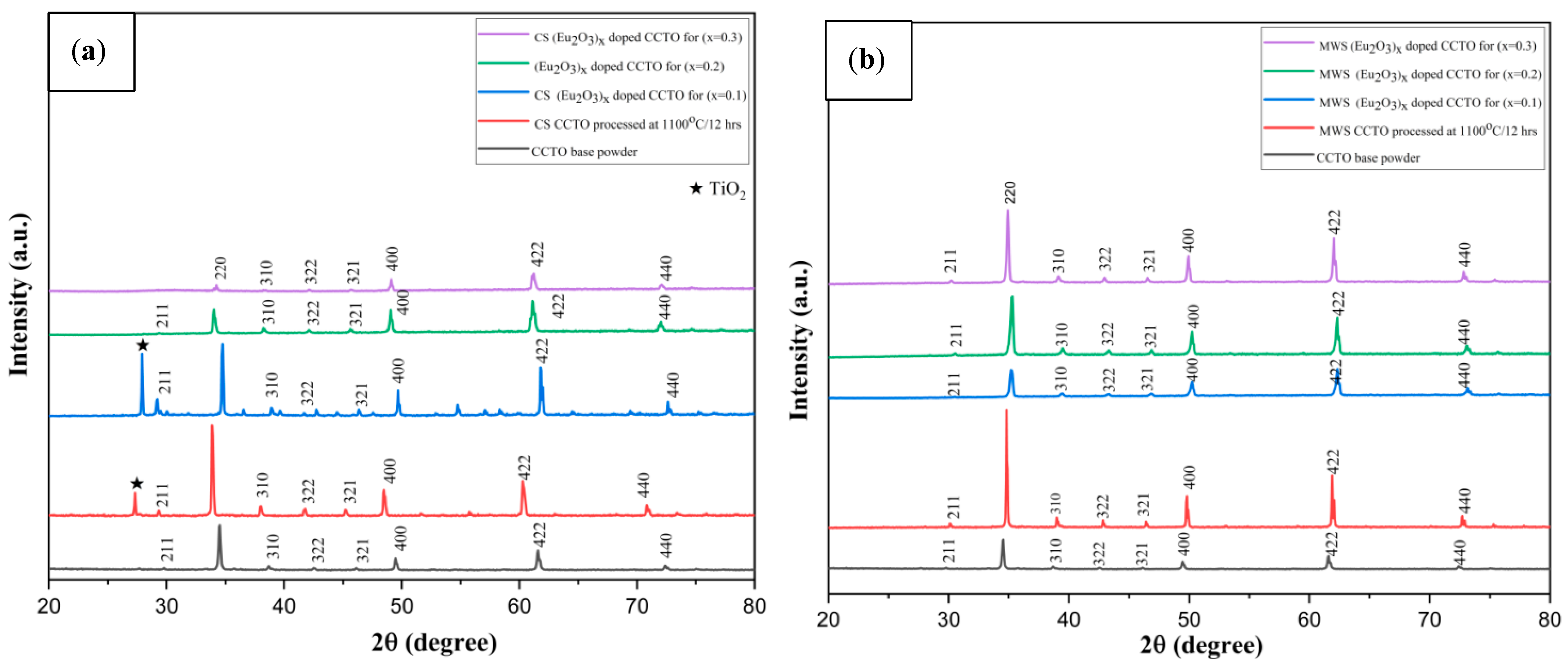
2.1. XRD Analysis
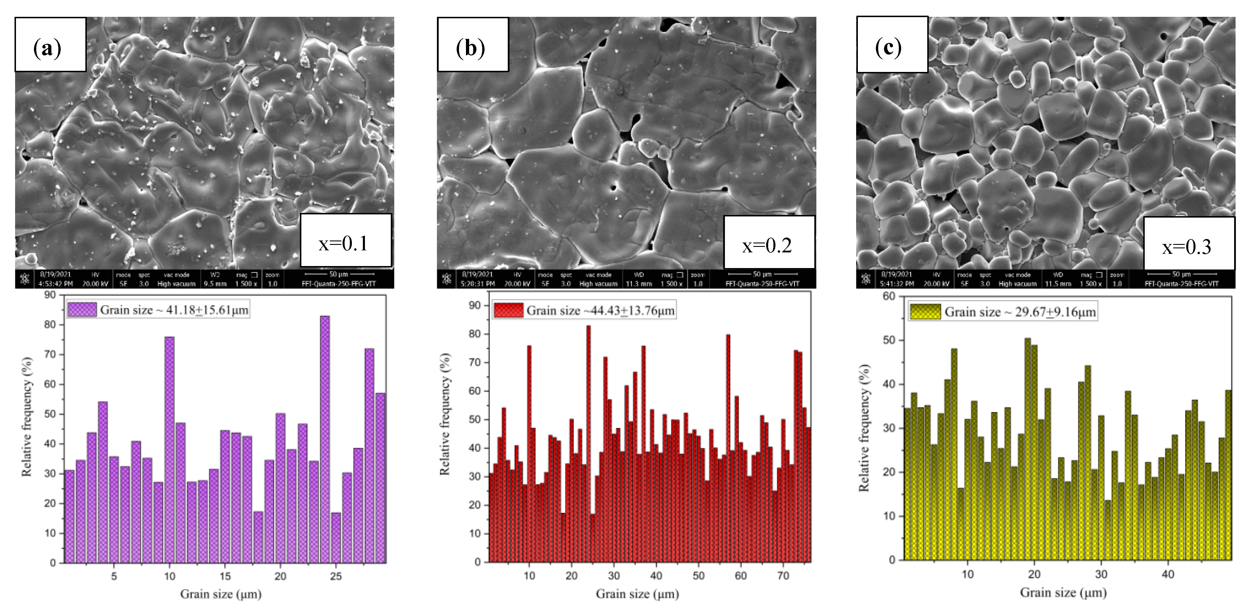
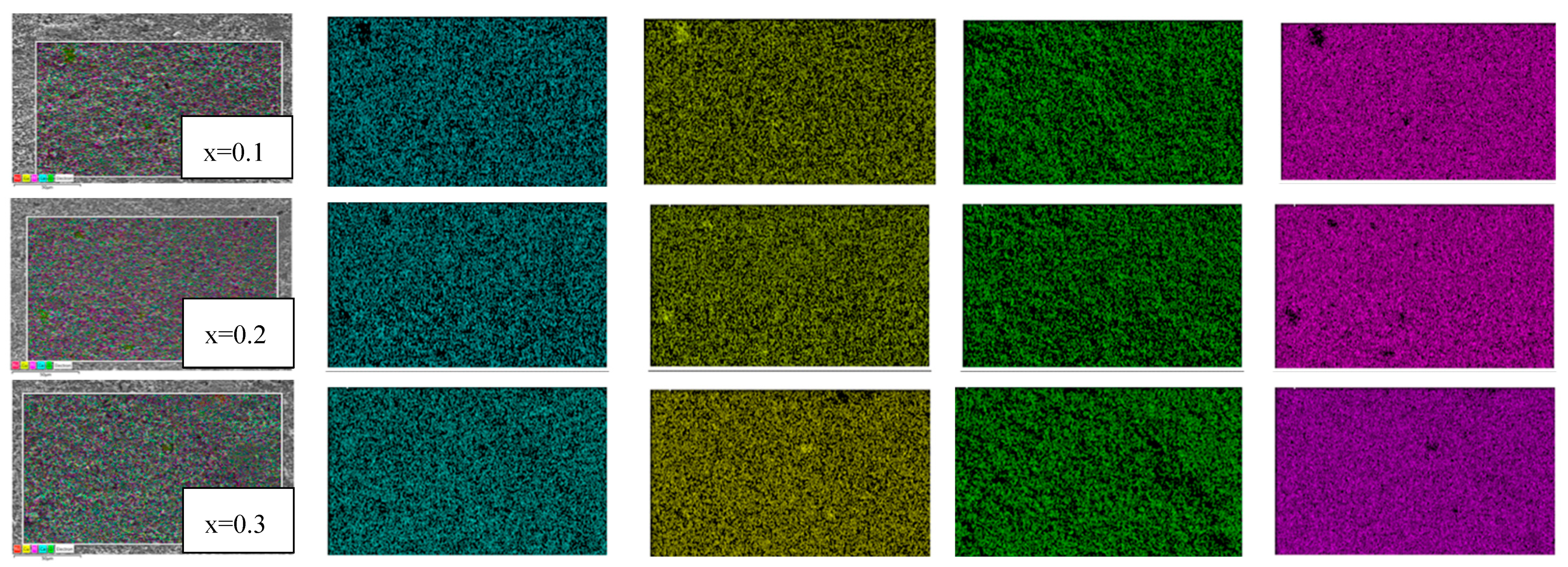
2.2. Microstructure Analysis Using SEM and EDS
2.3. X-ray Photoelectron Spectroscopy (XPS) Analysis
2.4. Dielectric Characteristics
3. Materials and Methods
3.1. Material Preparation
3.2. Sample Processing and Characterization
4. Conclusions
- The absence of Cu phase segregation at the grain boundaries was confirmed by XRD plots and elemental mapping. In addition, the evolution of microstructure fostered by the inclusion of europium in the CCTO structure led to smaller grains in the CS samples at x > 0.2 and elevated for MWS samples at x > 0.1. In the case of the absence of grain boundaries with different electro-chemical characters, the phenomena taking place at atomic lattice level are responsible for the dielectric behavior of samples.
- The charge compensation effect, which is facilitated by reduction processes, have been confirmed by XPS analysis for Ti4+ and Cu2+ that directly impacts the dielectric properties.
- The dielectric constant ε was greater than 104 and 102 for CS and MWS samples, with stable low tan δ at high frequencies ranging from 105 to 107 Hz. Although the presence of Eu3+ induces low tan δ at high frequencies, boosting the dielectric constant is dependent on a number of factors, which include the presence of oxygen vacancies, and the type and area of contact of the electrodes with the sample.
Author Contributions
Funding
Data Availability Statement
Acknowledgments
Conflicts of Interest
References
- Chung, S.-Y.; Kim, I.-D.; Kang, S.-J.L. Strong nonlinear current–voltage behaviour in perovskite-derivative calcium copper titanate. Nat. Mater. 2004, 3, 774–778. [Google Scholar] [CrossRef]
- Boonlakhorn, J.; Chanlek, N.; Manyam, J.; Srepusharawoot, P.; Krongsuk, S.; Thongbai, P. Enhanced giant dielectric properties and improved nonlinear electrical response in acceptor-donor (Al3+, Ta5+)-substituted CaCu3Ti4O12 ceramics. J. Adv. Ceram. 2021, 10, 1243–1255. [Google Scholar] [CrossRef]
- Liu, L.; Fang, L.; Huang, Y.; Li, Y.; Shi, D.; Zheng, S.; Wu, S.; Hu, C. Dielectric and nonlinear current–voltage characteristics of rare–earth doped CaCu3Ti4O12 ceramics. J. Appl. Phys. 2011, 110, 094101. [Google Scholar] [CrossRef]
- Tan, J.; Zhou, J.; Guo, Y.; Ren, F.; Jiang, P.; Zhao, J. Giant dielectric response and nonlinear electrical behaviors of TiO2/CCTO composite ceramics with pomegranate-like microstructure. Ceram. Int. 2022, 48, 27905–27912. [Google Scholar] [CrossRef]
- Tararam, R.; Bdikin, I.; Varela, J.; Bueno, P.R.; Kholkin, A.L. Local Electromechanical Properties of CaCu3Ti4O12 Ceramics. MRS Proc. 2010, 1255, 4. [Google Scholar] [CrossRef]
- Ramirez, A.; Subramanian, M.; Gardel, M.; Blumberg, G.; Li, D.; Vogt, T.; Shapiro, S. Giant dielectric constant response in a copper-titanate. Solid State Commun. 2000, 115, 217–220. [Google Scholar] [CrossRef]
- Subramanian, M.A.; Li, D.; Duan, N.; Reisner, B.A.; Sleight, A.W. High Dielectric Constant in ACu3Ti4O12 and ACu3Ti3FeO12 Phases. J. Solid State Chem. 2000, 151, 323–325. [Google Scholar] [CrossRef]
- Clark, J.H.; Dyer, M.S.; Palgrave, R.G.; Ireland, C.P.; Darwent, J.R.; Claridge, J.B.; Rosseinsky, M.J. Visible Light Photo-oxidation of Model Pollutants Using CaCu3Ti4O12: An Experimental and Theoretical Study of Optical Properties, Electronic Structure, and Selectivity. J. Am. Chem. Soc. 2010, 133, 1016–1032. [Google Scholar] [CrossRef] [PubMed]
- Wang, M.; Liu, J.; Xu, C.; Feng, L. Sonocatalysis and sono-photocatalysis in CaCu3Ti4O12 ceramics. Ceram. Int. 2022, 48, 11338–11345. [Google Scholar] [CrossRef]
- Chattopadhyay, A.; Nayak, J. Improvement of humidity sensing performance and dielectric response through pH variation in CaCu3Ti4O12 ceramics. Sens. Actuators A Phys. 2022, 341, 113603. [Google Scholar] [CrossRef]
- Bhardwaj, U.; Sharma, A.; Gupta, V.; Batoo, K.M.; Hussain, S.; Kushwaha, H.S. High energy storage capabilities of CaCu3Ti4O12 for paper-based zinc–air battery. Sci. Rep. 2022, 12, 3999. [Google Scholar] [CrossRef]
- Adams, T.; Sinclair, D.; West, A. Giant Barrier Layer Capacitance Effects in CaCu3Ti4O12 Ceramics. Adv. Mater. 2002, 14, 1321–1323. [Google Scholar] [CrossRef]
- Mao, P.; Wang, J.; Zhang, L.; Liu, S.; Zhao, Y.; Sun, Q. Rapid fabrication and improved electrical properties of CaCu3Ti4O12 ceramics by sol–gel and spark plasma sintering techniques. J. Mater. Sci. Mater. Electron. 2019, 30, 13401–13411. [Google Scholar] [CrossRef]
- Shao, S.F.; Zhang, J.L.; Zheng, P.; Zhong, W.L.; Wang, C.L. Microstructure and electrical properties of CaCu3Ti4O12 ceramics. J. Appl. Phys. 2006, 99, 084106. [Google Scholar] [CrossRef]
- Fang, T.-T.; Shiau, H.-K. Mechanism for Developing the Boundary Barrier Layers of CaCu3Ti4O12. J. Am. Ceram. Soc. 2005, 87, 2072–2079. [Google Scholar] [CrossRef]
- Bender, B.; Pan, M.-J. The effect of processing on the giant dielectric properties of CaCu3Ti4O12. Mater. Sci. Eng. B 2005, 117, 339–347. [Google Scholar] [CrossRef]
- Ramadan, R.M.; Labeeb, A.M.; Ward, A.; Ibrahim, A.M.H. New approach for synthesis of nano-sized CaCu3Ti4O12 powder by economic and innovative method. J. Mater. Sci. Mater. Electron. 2020, 31, 9065–9075. [Google Scholar] [CrossRef]
- Supriya, D.M.; Rajani, M.R.; Phani, A.R.; Naveen, C.V.S.; Ravishankar, R. Synthesis of CCTO and Doped CCTO Nanopowders and its Applications in the Field of Electronics. Mater. Today Proc. 2017, 4, 12021–12025. [Google Scholar] [CrossRef]
- Munir, Z.A.; Anselmi-Tamburini, U.; Ohyanagi, M. The effect of electric field and pressure on the synthesis and consolidation of materials: A review of the spark plasma sintering method. J. Mater. Sci. 2006, 41, 763–777. [Google Scholar] [CrossRef]
- Thomas, P.; Sathapathy, L.N.; Dwarakanath, K.; Varma, K.B.R. Microwave synthesis and sintering characteristics of CaCu3Ti4O12. Bull. Mater. Sci. 2007, 30, 567–570. [Google Scholar] [CrossRef]
- Evangeline, T.G.; Annamalai, A.R. Influence of heating modes on the microstructural and dielectric properties of calcium copper titanium oxide (CaCu3Ti4O12/CCTO) using conventional and microwave sintering. J. Mater. Sci. Mater. Electron. 2022, 33, 5806–5815. [Google Scholar] [CrossRef]
- Zhao, J.; Zhao, H.; Zhu, Z. Influence of sintering conditions and CuO loss on dielectric properties of CaCu3Ti4O12 ceramics. Mater. Res. Bull. 2019, 113, 97–101. [Google Scholar] [CrossRef]
- Kawrani, S.; Boulos, M.; Bekheet, M.F.; Viter, R.; Nada, A.; Riedel, W.; Roualdes, S.; Cornu, D.; Bechelany, M. Segregation of copper oxide on calcium copper titanate surface induced by Graphene Oxide for Water splitting applications. Appl. Surf. Sci. 2020, 516, 146051. [Google Scholar] [CrossRef]
- Xue, R.; Chen, Z.; Dai, H.; Liu, D.; Li, T.; Zhao, G. Effects of rare earth ionic doping on microstructures and electrical properties of CaCu3Ti4O12 ceramics. Mater. Res. Bull. 2015, 66, 254–261. [Google Scholar] [CrossRef]
- Mu, C.; Zhang, H.; Liu, Y.; Song, Y.; Liu, P. Rare earth doped CaCu3Ti4O12 electronic ceramics for high frequency applications. J. Rare Earths 2010, 28, 43–47. [Google Scholar] [CrossRef]
- Evangeline, T.G.; Annamalai, A.R. Dielectric properties of conventional and microwave sintered Lanthanum doped CaCu3Ti4O12 ceramics for high-frequency applications. Ceram. Int. 2022, 48, 25705–25713. [Google Scholar] [CrossRef]
- Subramanian, M.; Sleight, A. ACu3Ti4O12 and ACu3Ru4O12 perovskites: High dielectric constants and valence degeneracy. Solid State Sci. 2002, 4, 347–351. [Google Scholar] [CrossRef]
- Thongbai, P.; Putasaeng, B.; Yamwong, T.; Maensiri, S. Modified giant dielectric properties of samarium doped CaCu3Ti4O12 ceramics. Mater. Res. Bull. 2012, 47, 2257–2263. [Google Scholar] [CrossRef]
- Zhang, J.; Guo, S.; Lu, W.; Lei, Z.; Li, Y.; Tian, M. Differences between La substitution and doping strategies in dielectric properties of CaCu3Ti4O12 ceramics with low loss. J. Mater. Sci. Mater. Electron. 2022, 33, 7011–7022. [Google Scholar] [CrossRef]
- Li, M.; Liu, Q.; Li, C. Study of the dielectric responses of Eu-doped CaCu3Ti4O12. J. Alloy Compd. 2017, 699, 278–282. [Google Scholar] [CrossRef]
- Boonlakhorn, J.; Chanlek, N.; Suksangrat, P.; Thongbai, P.; Srepusharawoot, P. Colossal dielectric properties of Na1/3Ca1/3Sm1/3Cu3Ti4O12 ceramics: Computational and experimental investigations. Ceram. Int. 2023, 49, 1690–1699. [Google Scholar] [CrossRef]
- Boonlakhorn, J.; Prachamon, J.; Jumpatam, J.; Krongsuk, S.; Thongbai, P.; Srepusharawoot, P. Dielectric characteristics of a (Cd2+, F−) co-doped CaCu3Ti4O12/CaTiO3 binary system improved with increased dielectric permittivity and decreased dielectric loss tangent. Results Phys. 2022, 34, 105275. [Google Scholar] [CrossRef]
- Sinclair, D.C.; Adams, T.B.; Morrison, F.D.; West, A.R. CaCu3Ti4O12: One-step internal barrier layer capacitor. Appl. Phys. Lett. 2002, 80, 2153–2155. [Google Scholar] [CrossRef]
- Kwon, S.; Huang, C.-C.; Subramanian, M.; Cann, D.P. Effects of cation stoichiometry on the dielectric properties of CaCu3Ti4O12. J. Alloy Compd. 2009, 473, 433–436. [Google Scholar] [CrossRef]
- Subramanian, M.; Marshall, W.; Calvarese, T.; Sleight, A. Valence degeneracy in CaCu3Cr4O12. J. Phys. Chem. Solids 2003, 64, 1569–1571. [Google Scholar] [CrossRef]
- Kumari, N.; Meena, S.; Rathore, D.; Singhal, R.; Dwivedi, U.K. Study of dielectric properties of CaCu3Ti4O12 synthesized via different routes: Effect of sintering temperature. Ceram. Int. 2023, 49, 2549–2556. [Google Scholar] [CrossRef]
- Liu, J.; Lu, D.-Y.; Yu, X.-Y.; Liu, Q.; Tao, Q.; Change, H.; Zhu, P.-W. Dielectric Properties of Eu-Doped CaCu3Ti4O12 with Different Compensation Mechanisms. Acta Met. Sin.Engl. Lett. 2016, 30, 97–103. [Google Scholar] [CrossRef]
- Yang, J.; Shen, M.; Fang, L. The electrode/sample contact effects on the dielectric properties of the CaCu3Ti4O12 ceramic. Mater. Lett. 2005, 59, 3990–3993. [Google Scholar] [CrossRef]
- Zhang, L. Electrode and grain-boundary effects on the conductivity of CaCu3Ti4O12. Appl. Phys. Lett. 2005, 87, 022907. [Google Scholar] [CrossRef]


Disclaimer/Publisher’s Note: The statements, opinions and data contained in all publications are solely those of the individual author(s) and contributor(s) and not of MDPI and/or the editor(s). MDPI and/or the editor(s) disclaim responsibility for any injury to people or property resulting from any ideas, methods, instructions or products referred to in the content. |
© 2023 by the authors. Licensee MDPI, Basel, Switzerland. This article is an open access article distributed under the terms and conditions of the Creative Commons Attribution (CC BY) license (https://creativecommons.org/licenses/by/4.0/).
Share and Cite
Evangeline T, G.; Annamalai A, R.; Ctibor, P. Effect of Europium Addition on the Microstructure and Dielectric Properties of CCTO Ceramic Prepared Using Conventional and Microwave Sintering. Molecules 2023, 28, 1649. https://doi.org/10.3390/molecules28041649
Evangeline T G, Annamalai A R, Ctibor P. Effect of Europium Addition on the Microstructure and Dielectric Properties of CCTO Ceramic Prepared Using Conventional and Microwave Sintering. Molecules. 2023; 28(4):1649. https://doi.org/10.3390/molecules28041649
Chicago/Turabian StyleEvangeline T, Gecil, Raja Annamalai A, and Pavel Ctibor. 2023. "Effect of Europium Addition on the Microstructure and Dielectric Properties of CCTO Ceramic Prepared Using Conventional and Microwave Sintering" Molecules 28, no. 4: 1649. https://doi.org/10.3390/molecules28041649