

Abstract
Silicene, a monolayer of silicon atoms arranged in a honeycomb lattice, is excellently compatible with the materials used in today's semiconductor manufacturing. In this paper, silicene-terminated CaSi2 is cleaved inside a transmission electron microscope using an in situ manipulator. HRTEM studies on a standard lift-out lamella performed from several crystallographic orientations confirm the cell parameters of a = 3.7 Å and c = 30.60 Å, and allow to determine its exact orientation in the SEM/FIB system. A FIB procedure with corrected tilting and rotating angles has been developed to ensure that the tensile force applied by the manipulator is perpendicular to the (0 0 1) plane, and that the [1 0 0] pole axis could be used for HRTEM imaging. A sharp and flat cleavage interface with a length of more than 1 μm was observed in one in situ experiment. HRTEM images from multiple regions confirm that the flat cleavage follows the (0 0 3) plane of the CaSi2 crystal. The current in situ study demonstrates that a surface sheet with silicene-like atomic arrangement can be mechanically exfoliated from silicide compounds.
Export citation and abstract BibTeX RIS
1. Introduction
The groundbreaking work on graphene in 2004 [1] has initiated an unprecedented boom in 2D materials research. Due to their superior properties, 2D materials promise tremendous potential applications in electronics, optoelectronics, membranes, energy storage and generation, catalysis, sensing and so on [2]. Silicene [3], i.e. a monolayer of silicon atoms arranged in a honeycomb lattice, is excellently compatible with the materials used in today's semiconductor manufacturing. However, lack of controlled ways to obtain these corrugated, sp3 bonded silicon atoms in one sheet hinders its application in devices. In addition, the silicon atoms tend to be oxidized once they are exposed in air already after a very short time. Therefore, much effort has to be spent exploring methods to produce high-quality silicene.
So far, silicene nanoribbons and highly ordered sheets have been grown mainly on metal substrates, i.e. Ag (1 1 0) [4, 5], Ag (1 1 1) [6, 7], Au (1 1 0) [8], Ir (1 1 1) [9] and Pt (1 1 1) [10]. Non-metallic substrates including ZrB2 and LaAlO3 have been recently reported to grow silicene [11, 12]. A few attempts using chemical exfoliation techniques have been made to isolate silicene from silicide compounds as well [3, 13–15]. Compared to graphene, fabrication techniques for silicene are still not developed well enough to explore its potential for further applications. This is important for a more comprehensive study of the physical characteristics and properties experimentally. Mechanical exfoliation has been used successfully to extract highest quality of graphene from highly oriented pyrolytic graphite, however, has not been reported so far to fabricate silicene. In this study, an in situ manipulator inside a transmission electron microscope (TEM) is used to mechanically cleave silicene-terminated calcium disilicide (CaSi2) and to test the potential of mechanically exfoliating silicene sheets from silicide compounds.
2. Experimental section
Bulk CaSi2 samples were prepared by arc melting of a powder mixture of elements in stoichiometric ratio. The crystal structure is shown in figure S1 is available online at stacks.iop.org/NANO/31/095702/mmedia, it contains layered silicene with a buckled honeycomb structure. The experiment aims to pull the CaSi2 crystal along the [0 0 1] axis and to cleave the interface between the Si layer and the Ca layer. The sample was crushed by hand, and flat plateaus were generated as shown in figure 1(a). A standard lift-out lamella was fabricated from the plateau applying the standard technique with a tilt-angle of 54° during FIB milling (figures S2-4) in a SEM/FIB tool (Carl Zeiss NVision 40). The lamella was extracted along the direction parallel (indicated by the arrow in figure 1(a)) to the cracks on the plateau. The lift-out lamellae for in situ test were fabricated using a modified FIB procedure with corrected tilting and rotating angles as shown in figure S5. This procedure is crucial to ensure that the tensile force applied by the push-to-pull (PTP) device is perpendicular to the (0 0 1) plane of CaSi2. A high-resolution TEM image (a TEM Carl Zeiss Libra 200 Cs MC was used) acquired from [1 0 0] axis and the corresponding FFT pattern are shown in figure S6. The procedure to transfer the lamella to the PTP device is shown in figures 1(c)–(e). Firstly, a relative thick lamella was prepared using FIB milling. Afterwards, one side of the lamella was attached to the nanomanipulator, and the other side was cut free. The lamella was thinned down to about 150 nm before it was placed right on top of the 2.5 μm gap. The lamella was fixed on the PTP device at the upper and lower part by Pt deposition. The sample on the PTP device was mounted to the in situ mechanical testing holder (Bruker Picoindenter PI 95), and subsequently, it was transferred into the TEM.
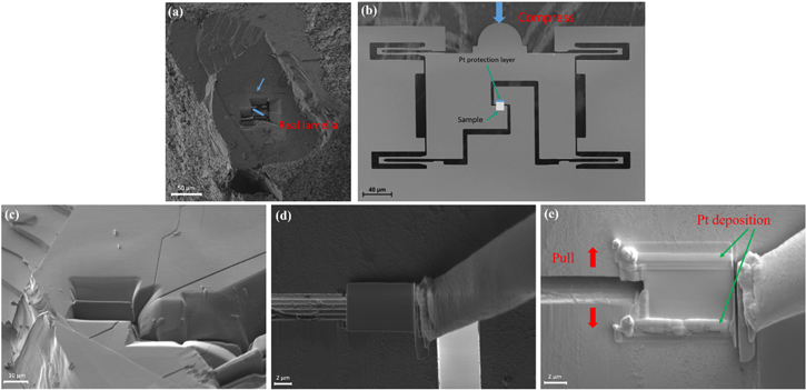
Figure 1. (a) SEM image of the CaSi2 phase (top view), (b) SEM image of the PTP device with a sketched lift-out lamella, (c) SEM image of a lamella (left) before lifting out, (d) the same lamella attached on the nanomanipulator on top of the PTP device, (e) SEM image of the fixed lift-out lamella.
Download figure:
Standard image High-resolution image3. Results and discussion
The standard lift-out lamella was tilted using α-tilt (tilted along the longitudinal direction of the holder) of the TEM holder only to determine the incident directions (figure S2). Series of HRTEM images acquired from several incident axes are shown in figure 2, and the vectors in reciprocal space are indexed in the corresponding FFT patterns. The lattice parameters derived from the HRTEM data are a = 3.7 Å and c = 30.60 Å, which are consistent with the data published in [3]. The information about the tilting series is summarized in table 1. The second column from the left lists the real angle recorded in the goniometer for each high resolution image, and the zone axis shows the indexed incident directions for each image. The last columns list the measured angle difference between two zone axes as obtained from the goniometer reading and as calculated from the lattice parameters and the tilt axis, showing good agreement. That means, the plane of the standard lift-out lamella is not perpendicular to the (0 0 1) plane, but it is tilted by an angle of 14.6° from (1 −2 0) plane. Due to the design of the in situ mechanical test setup and the PTP device inside the TEM holder, the plane of a lift-out lamella has to be perpendicular to the (0 0 1) plane of CaSi2 for the mechanical cleavage experiment. Therefore, a modified FIB procedure with corrected tilting and rotating angles described in figure S5 was introduced.
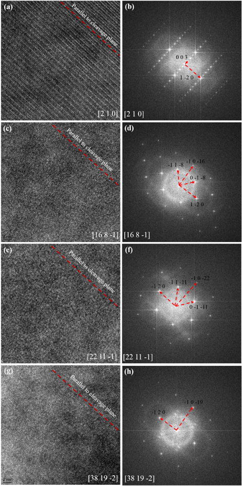
Figure 2. HRTEM images acquired from several incident directions, and the corresponding FFT patterns. (a) and (b) [2 1 0], (c) and (d) [16 8 −1], (e) and (f) [22 11 −1], (g) and (h) [38 19 −2].
Download figure:
Standard image High-resolution imageTable 1. Angles summarized from the tilting series shown in figure 2.
| α-tilt (°) | Zone axis | Angle | Angle-goniometer (°) | Angle-calculation (°) | |
|---|---|---|---|---|---|
| 1 | −14.6 | [2 1 0] | [2 1 0] v [16 8 −1] | 29.6 | 29.8 |
| 2 | +15 | [16 8 −1] | [16 8 −1] v [22 11 −1] | 7.0 | 7.2 |
| 3 | +8 | [22 11 −1] | [2 1 0] v [22 11 −1] | 22.6 | 22.6 |
| 4 | +11 | [38 19 −2] | [2 1 0] v [38 19 −2] | 25.6 | 25.7 |
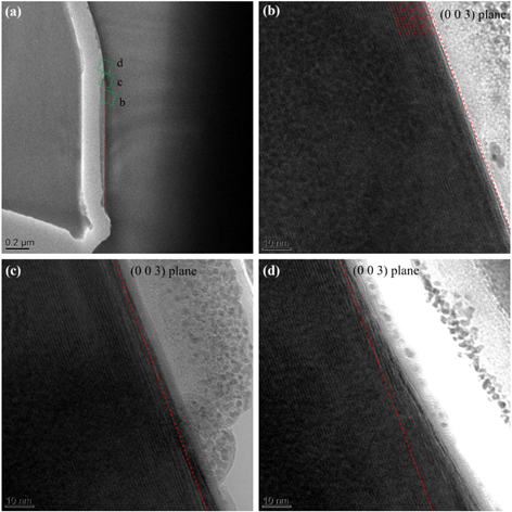
While the thin CaSi2 lamella on the PTP device was cleaved in the TEM using a 'PTP' principle [16], sequential images were recorded. The [1 0 0] incident axis (figure S6) was used for imaging of the lamella, and the tensile force applied by a PTP device was perpendicular to the (0 0 1) plane of the CaSi2. The video from an experiment is shown in Video S1. The change of fringes on the surface indicates that the lamella was strained until fracture. Two FIB cuts in the middle were used to initialize the cleavage in the middle instead of in the region where Pt was deposited (figure S7). The cleavage in the Pt deposited region would generate an unsmooth surface due to the modified microstructure of CaSi2 by the ultra-high dose of Ga ions in the deposition process for fixing the lamella on the PTP device, and the broken interface does not follow a preferred plane (e.g. (0 0 1) plane). A sharp and flat cleavage interface (red dashed line) with a length of more than 1 μm was fabricated as shown in figure 3(a). The thickness of the flat cleavage was about 150 nm from previous FIB milling process. After the in situ experiment, the cleaved sample was made on hold using piezo control on the TEM holder. The stationary sample with the area of interest was zoomed in by increasing the magnification and illumination step in the TEM until reaching the satisfied HRTEM imaging. HRTEM images from multiple regions (marked by a green square box) at the cleavage interface were recorded (figures 3(b)–(d)). The HRTEM images confirm that the flat cleavage followed the (0 0 3) plane of the CaSi2 crystal, and the tilted cleavage followed a curved path with continuously changed angles from (0 0 3) plane. Recently, calculations of the cleavage energy showed that silicene-termined bulk CaSi2 is in favor of cleavage perpendicular to [0 0 1], and the silicene layer should remain undivided [17]. To our best knowledge, our results for the first time experimentally confirm the potential to mechanically exfoliate silicene from silicide. Another point worth noting is that a thin layer torn on the surface of the 150 nm lamella shows an interface with random orientation/no preferred orientation (indicated by arrows in figure S8). It indicates that it would be very difficult to create a flat cleavage along a fixed plane in very thin sample. Therefore, a certain thickness of the lamella is recommended to produce a flat cleavage along the (0 0 1) plane. Due to the extreme complexity of sample preparation, and handling in the transfer process and in situ experiment, it is still very challenging to controllably cleave silicene surface from CaSi2 in our approach. However, the possibility of mechanical exfoliation to obtain silicene surface is experimentally confirmed in current study. More feasible mechanical exfoliation methods should be developed further in order to achieve big size of silicene applicable for device applications. Another direction could be synthesizing novel silicene-containing compound with weak interface, which could facilitate the exfoliation process. For example, the SEM image of CaSi2Fx compound published in [18] already showed natural macroscopic flat cracks after synthesis.
Figure 3. (a) Cleaved CaSi2 lamella after in situ test, (b)–(d) HRTEM image of the area marked by the green square box.
Download figure:
Standard image High-resolution image
4. Conclusions
An in situ methodology was developed to cleave a silicene-terminated bulk CaSi2 phase inside the TEM. HRTEM studies on a standard lift-out lamella at several incident axes using α-tilting reveal the cell parameters of the CaSi2 phase of a = 3.7 Å and c = 30.60 Å; more importantly determined the exact orientation in real space for the samples used in the SEM/FIB tool, which is the most crucial prerequisite for the sample preparation in the in situ test. A dedicated FIB procedure with corrected tilting and rotating angles was adopted to ensure that the tensile force applied by the PTP device was exactly perpendicular to the (0 0 1) plane of the CaSi2. The [1 0 0] incident axis was used for imaging the lamella in the TEM. The thin lamella was transferred and fixed to the PTP device through a dedicated procedure, and was mounted on a TEM holder. A sharp and flat cleavage interface with a length of more than 1 μm was generated in an in situ experiment. HRTEM images from multiple regions confirm that the flat cleavage follows the (0 0 3) plane of the CaSi2 crystal, and the tilted cleavage follows a curved path with continuously changing angles from (0 0 3) plane. The in situ observation of the cleaving experiment and HRTEM studies on the cleavage interface confirm the potential of mechanically exfoliating silicene from silicide compounds.
Acknowledgments
Funding by the German Research Foundation (project number: 267459210) and Czech Science Foundation (project number 15-08842 J) is gratefully acknowledged.