
Synthesis and Pressure-Assisted Sintering of CaCu3Ti4O12 Dielectrics


1
Faculty of Electrical Engineering, Czech Technical University, Technická 2, 166 27 Prague, Czech Republic
2
Institute of Plasma Physics, The Czech Academy of Sciences, Za Slovankou 3, 182 00 Prague, Czech Republic
*
Author to whom correspondence should be addressed.
Ceramics 2021, 4(3), 447-466; https://doi.org/10.3390/ceramics4030033
Submission received: 15 April 2021
/
Revised: 29 April 2021
/
Accepted: 5 August 2021
/
Published: 9 August 2021
(This article belongs to the Special Issue Innovative Processing Routes for Electroactive Materials)
Abstract
:In this paper, we examined the dielectric properties of CaCu3Ti4O12 (CCTO) ceramics fabricated by various routes and discussed the most important conditions affecting their dielectric behavior. We prepared feedstock powder using a molten salt route and compared it with a commercial powder. Both powders were sintered using SPS. For some samples, annealing was applied after sintering. Other samples were obtained by high-pressure forming and conventional sintering, using both powders. Phase composition, porosity and microhardness were evaluated in comparison with the literature. The results showed that a sintering temperature just below or equal to 1000 °C should be set for the SPS process. However, the best dielectric characteristics were obtained in samples prepared by high-pressure forming and conventional sintering, which showed a relative permittivity of 22,000 and a loss tangent of 0.13 at 1 MHz.
1. Introduction
Ceramic capacitors represent one of the basic electronic components. While some materials show appropriate properties, scientists still examine new materials, or new combinations of existing ones, in order to obtain improved electrical properties. Some examples of such materials are represented by doped-BaTiO3, doped-TiO2, CaCrTi2O6 and CaCu3Ti4O12, which show comparatively high, so-called giant, values of relative permittivity (εr = 104 or higher) [1,2]. One of the reasons why CaCu3Ti4O12 (CCTO) gained our attention was because our previous research was focused on various unconventional forms of titanates, such as plasma-sprayed thick films and spark-plasma sintered bulks. These titanates usually belong to the perovskites group, which has a general formula of ABO3, with BaTiO3 and CaTiO3 being typical prototypes. Analogously, the compounds CaCrTi2O6 and CaCu3Ti4O12 are often categorized as double and quadruple perovskites, respectively. It is interesting to examine the mechanisms standing behind their high relative permittivity (dielectric constant as high as 20,000 for ceramics and 300,000 for single crystals [3]), also because a single theory that describes these outstanding values has not been established [3]. The giant dielectric response of CCTO is unlikely related to intrinsic properties, i.e., perfectly stoichiometric, defect-free single crystals. For polycrystalline samples, influential defects lie at grain boundaries, including dislocations and planar defects, e.g., stacking faults. While some authors ascribe the colossal dielectric response to the lattice structure of the material [4,5], and some to the depletion layer between the sample and the electrodes [6], the most widely accepted theory explains the colossal permittivity with an internal barrier layer capacitance (IBLC) [7,8]. The IBLC could be further divided into macroscale barrier layer capacitance (MBLC) and nanoscale barrier layer capacitance (NBLC) [9]. Occasionally, it is reported, that the high dielectric constant might be related to the high electrical conductivity [5], which is also mediated by oxidation. Heavy oxidation on the sample surfaces could occur during annealing in air. It has been found that 1020 °C is the optimal annealing temperature to maximize the dielectric constant of CCTO [10]. Upon annealing, the grain boundaries oxidize faster than the bulk of the grain, lowering their electrical conductivity compared to that of the bulk grains.
CCTO ceramics can be synthesized via various routes. Solid-state reaction is probably the most straightforward process [11], requiring a well-homogenized mixture of the input materials to be kept at high temperatures (above 1000 °C). The whole process requires a relatively long time (over 8 h). In the following text, we describe the chemical synthesis of the powder suitable for processing compact ceramic bodies by spark plasma sintering technique. Spark plasma sintering (SPS) enables very rapid fabrication of bulk ceramic materials. It is an emerging consolidation technique that combines pulsed electric currents with uniaxial pressure-induced compaction. High heating rate, mechanical pressure and pulsed current patterns are the main factors responsible for the enhancement of densification kinetics and fine-grained microstructures [12]. SPS has been often used for processing dielectric ceramics, although it may cause structural disorder [13] that can also affect the dielectric properties [12,14]. The SPS process is fast (usually completed within minutes) and can successfully hinder grain growth in dielectric ceramics [15]. By applying mechanical pressure during an appropriate thermal cycle, fully dense ceramics with fine grain size between 50 and 100 nm can be obtained [16]. The goals of the present study are the following:
- -
- To synthesize the CCTO feedstock powder via the molten salt route;
- -
- To compare the use of the SPS process and the SPS-related modification of a conventional sintering process (labeled HPF) on the microstructure of CCTO compacts;
- -
- To compare the dielectric properties of the fired CCTO bulks obtained from different powders sintered by different methods.
Based on these comparisons, we show that the newly developed HPF process enables avoiding the main drawbacks of SPS and conventional sintering. These include: (i) the contamination of CCTO with graphite occurring during SPS; (ii) the high internal stress in samples sintered by SPS; (iii) possible residua of plasticizers from the green body after conventional sintering; (iv) long dwell time at the firing temperature commonly used in conventional sintering.
2. Materials and Methods
2.1. Sample Preparation
The powder synthesis was carried out using the molten salt method. Compared to the traditional solid-state process, molten salt requires significantly lower temperatures and shorter sintering times. Additionally, it also tolerates a certain level of heterogeneity in the initial mixture due to higher mobility in the liquid state, which leads to an enhanced mixing of the components at the molecular scale [17]. On the other hand, the subsequent salt extraction is time-consuming, and the formation of specific compounds may result in undesired side products, e.g., Na2Ti6O13 in the case of CCTO. While a range of salts can be used, we decided to select NaCl, mainly because it does not require any precautions, and it can be easily acquired in laboratory grade. The following additional starting components have been selected: CaCO3 (99% purity, Sojuzchimexport), CuO (99%, Alfa Aesar) and TiO2 (99%, Alfa Aesar), which were all obtained in powder form. These powders were weighted according to the stoichiometry, mixed and blended in ethanol by a hand stirrer for approximately 15 min. The ethanol was then evaporated, and sodium chloride (laboratory grade, Verkon) was added to the mixture, which was inserted into a refractory crucible, heated in a resistance furnace and kept for 2 h at 820 °C. After cooling, distilled water was poured through the product (5 to 10 times on average) so that the dissolved sodium chloride could be washed out. One possible way to check whether NaCl is removed is to measure the electrical resistance of water before and after each washing cycle using a fixed setup. Since this method was later proved to be sufficiently reliable to estimate the state of the reaction process, it has been used throughout this work. NaCl was considered to be removed from the product when the conductance of water rose by two orders of magnitude. The CCTO powder synthesized with this process is here indicated as P1. A commercial powder (American Elements, Los Angeles, CA, USA), here labeled P2, was purchased as an alternative source of the feedstock. The info datasheet provided by the producer stated that the “average particle size” is below 5 µm. Both powders were subjected to X-ray diffraction analysis before sintering (Figure 1). The powder was sintered in an evacuated chamber of the SPS machine (10–4, Thermal Technology LLC, Santa Rosa, CA, USA), with processing parameters shown in Figure 2. The resulting samples were cylindrical with 20 mm in diameter and 4 to 5 mm in height. Subsequent annealing of the samples was carried out in air in a laboratory furnace using two regimes. In both regimes, a heating and cooling rate of 7 °C/min was previously set. The annealing temperature was set to 900 °C in the first case and 1000 °C in the second. The dwell time was the same for both, i.e., 30 min. The annealing temperature was chosen on the basis of the thermal analysis results to remove the carbon contamination. This approach allowed us to observe the effects of the annealing process on the microstructure and properties of CCTO.
Because of the repeated presence of carbon in the SPS samples (diffused from the SPS punches and die) and of the strong chemically reducing conditions during SPS, we focused on the development of alternative processing routes to produce high-quality CCTO dielectrics by applying the lowest possible thermal load (combination of low sintering temperature and short sintering time). As an alternative approach, we applied high-pressure forming before conventional sintering. This approach, here labeled as HPF, enabled us avoiding the addition of a plasticizer before the green body formation. A mechanical force corresponding to a constant pressure of 300 MPa was applied by the SPS apparatus at room temperature. Stainless-steel die and punches were used, and the as-formed tablets were removed from the punch/die assembly by a slow movement in a manual press. The movement had to be very delicate to avoid jamming. These compressed tablets were placed into a standard laboratory furnace and sintered in air. Because of the pronounced shrinkage in this case, the produced samples were cylinders with 17 to 18 mm in diameter and 4 to 5 mm in height. The whole set of experiments is schematically shown in Figure 3. The term “slow cooling” indicates the values of 10 °C/min and 2 °C/min for SPS and HPF, respectively. Analogously, the label “normal cooling“ refers to 100 °C/min for SPS and 7 °C/min for HPF.
2.2. Characterization
2.2.1. Phase Composition
The phase composition and lattice parameters were evaluated and compared by means of X-ray diffraction (XRD), carried out by the D8 Discover powder diffractometer in Bragg-Brentano geometry with a 1D detector and Cu-Kα radiation (scanned region from 20 to 130° 2θ with a 0.03° 2θ step size and a 192 s counting time per step). The obtained diffraction patterns were subjected to quantitative Rietveld analysis [18,19] performed using TOPAS 5 software, which utilizes the fundamental parameters approach [20].
2.2.2. Microstructure, Porosity and Mechanical Properties
The SEM micrographs and the chemical composition of the samples inspected by energy-dispersive X-ray microanalysis (EDX) were obtained by a desktop scanning electron microscope Phenom ProX (Phenom-World, Eindhoven, The Netherlands). The porosity of selected sintered compacts was estimated from the cross-sectional optical micrographs taken by a digital camera using Lucia G software (Laboratory Imaging, Czech Republic). The values reported are averages calculated from 10 frames analyzed at 250 times magnification. In addition to the simple porosity quantification, other factors were also examined. These include the size of individual pores expressed as “equivalent diameter” (E.D.), and the “circularity” of pores (i.e., 2D sections of 3D objects), which is equal to zero for a line and to one for a circle. The latter parameter correlates with the fact that samples fired by SPS sometimes contain flattened pores parallel to the surface as a result of the applied pressure. The number of pores per mm2 was recalculated from much smaller areas of the micrographs, typically about 50,000 µm2. The microhardness of the samples was measured using a Hanemann microhardness head (Zeiss, Germany) mounted on an optical microscope with a fixed load of 1 N and a Vickers indenter. Twenty indentations made on randomly selected areas on the cross-section of each sample were analyzed. Apparent density and open porosity of fired compacts were measured by the Archimedean (i.e., water immersion) method. The precision of these measurements is ±0.002 g/cm3 for the apparent density and about ±0.1% for the open porosity. Mercury intrusion porosimetry tests were performed by Auropore IV (Micromeritics, USA). A low-pressure analysis was carried out from 0.01 MPa to 0.25 MPa. This means that pore radii from 100 µm to 3 µm were analyzed. A high-pressure chamber was used for high-pressure analysis from 0.25 MPa to 400 MPa, covering the range of pore radii from 3 µm down to 1.5 nm. During the analysis, the applied pressure was increased stepwise up to the desired value, and the Hg volume penetrating the pores was measured. The pore size distribution was gained from these data (pressure and corresponding value of intrusion volume).
2.2.3. Dielectric Characterization
The dielectric parameters of the CCTO ceramics prepared by different methods were compared. For the SPS and HPF specimens, the dielectric properties were measured on as-fired samples. The opposite faces of the cylindrical samples were covered with aluminum in an evaporating apparatus. Using a mask, a system of three electrodes was applied to diminish the stray current effect during the measurements. One face was entirely coated, while the other one had an internal circle electrode of 12 mm diameter and an external ring electrode (ground-connected during the measurements), separated from the internal ring with a 1 mm wide gap. Before placing the electrodes, the samples were ground with SiC papers to eliminate surface unevenness. The electric field was applied along the same direction of the pressure applied during sintering (i.e., perpendicular to the cylinder face). The capacitance of the samples was measured using a programmable impedance analyzer model 4284A (Agilent, Santa Clara, CA, USA) and a high-precision sample fixture 16451B (Agilent, USA). The relative permittivity εr was calculated from the measured capacitance and specimen dimensions using the equation εr = (C·d)/(A·ε0), where C (F) is the electrical capacitance of the sample, d (m) is the sample thickness, A (m2) is the area of the measuring electrode and ε0 is the permittivity of vacuum (8.854 × 10⁻¹² F/m). The same equipment was also used for the loss tangent (Tan δ) measurement. Measurements at elevated temperatures were carried out using a programmable furnace Novotherm (Novocontrol, Montabaur, Germany). The DC volume resistance was measured on the same non-annealed samples used for the capacitance measurements, using a Keithley 6517B high resistance meter. The applied voltage for all resistance measurements was set to 50 ± 0.2 V. Customized Keithley 6104 shielded test enclosure was used to avoid errors from any external noise. The resistivity was calculated from the measured resistance and specimen dimensions using the equation: ρ = (R·A)/d, where R (Ω) is the electrical resistance, A (m2) is the area of the measuring electrode and d (m) the sample thickness.
3. Results and Discussion
3.1. Custom Synthesized and Commercial Powders
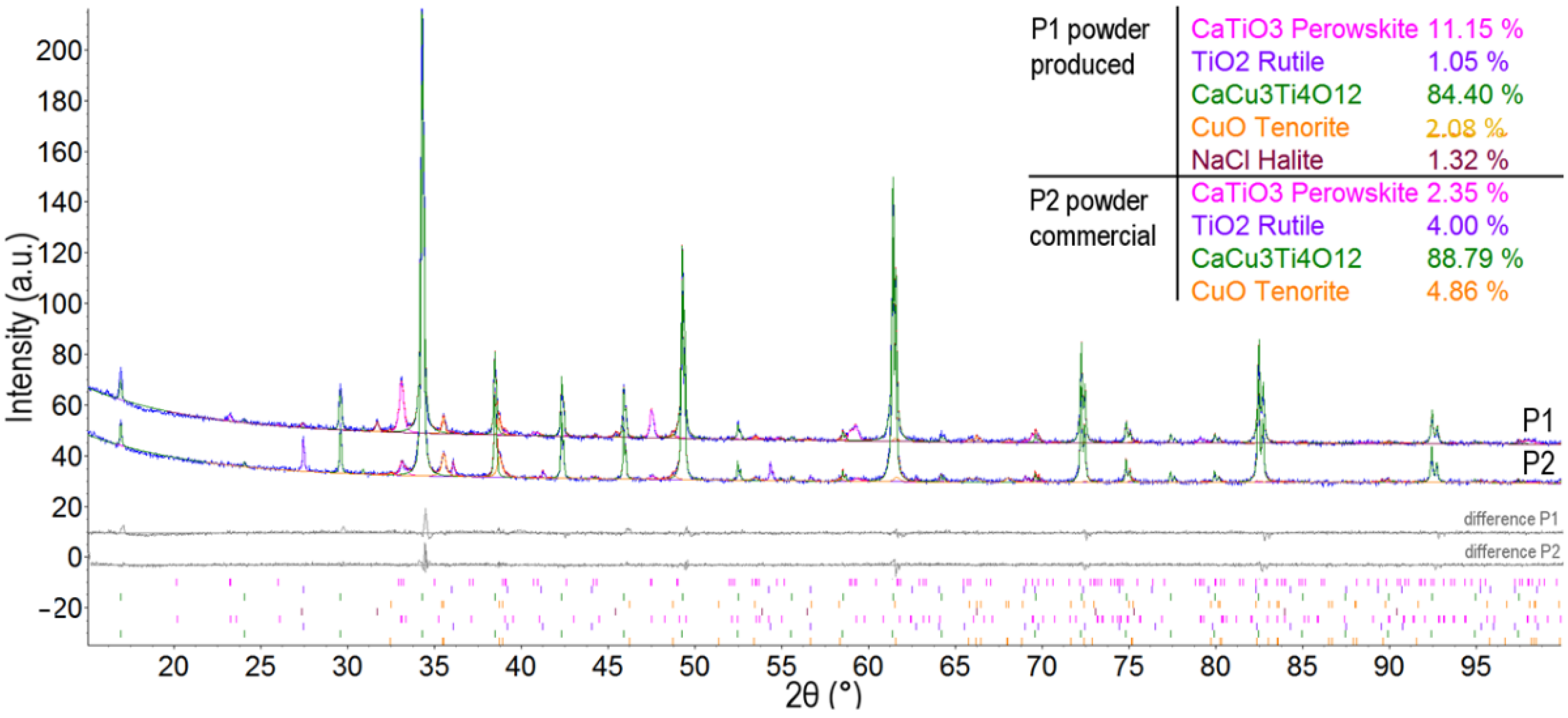
Figure 1 displays the X-ray diffraction pattern of the powder P1 prepared by the molten salt route. The first attempt had a success rate of just around 10%, while the following experiments ended with significantly better outcomes–over 80% of the desired CCTO phase. The rest of the materials consisted mainly of the CaTiO3 phase. The phase purity of the starting powder is one of the several criteria that need to be optimized to fabricate high-quality dielectric materials. An increased CuO content alters the conductivity at the grain boundaries [11] and is responsible for the formation of the IBLC under extended sintering times, resulting in low dielectric losses [3] since the grain boundaries occupied by CuO are thin. The quantity of about 1% of NaCl halite found in the powder P1 represents the unreacted amount from the synthesis input. The diffraction pattern of the commercial powder P2 is shown in Figure 1 as well. Its phase purity is comparable with that of powder P1. The CCTO content was nearly 90%, but besides CCTO and CaTiO3, it also contained significant proportions of TiO2 rutile and CuO tenorite phases. The presence of rutile is particularly undesired because of its high sintering temperature.
3.2. SPS Parameters
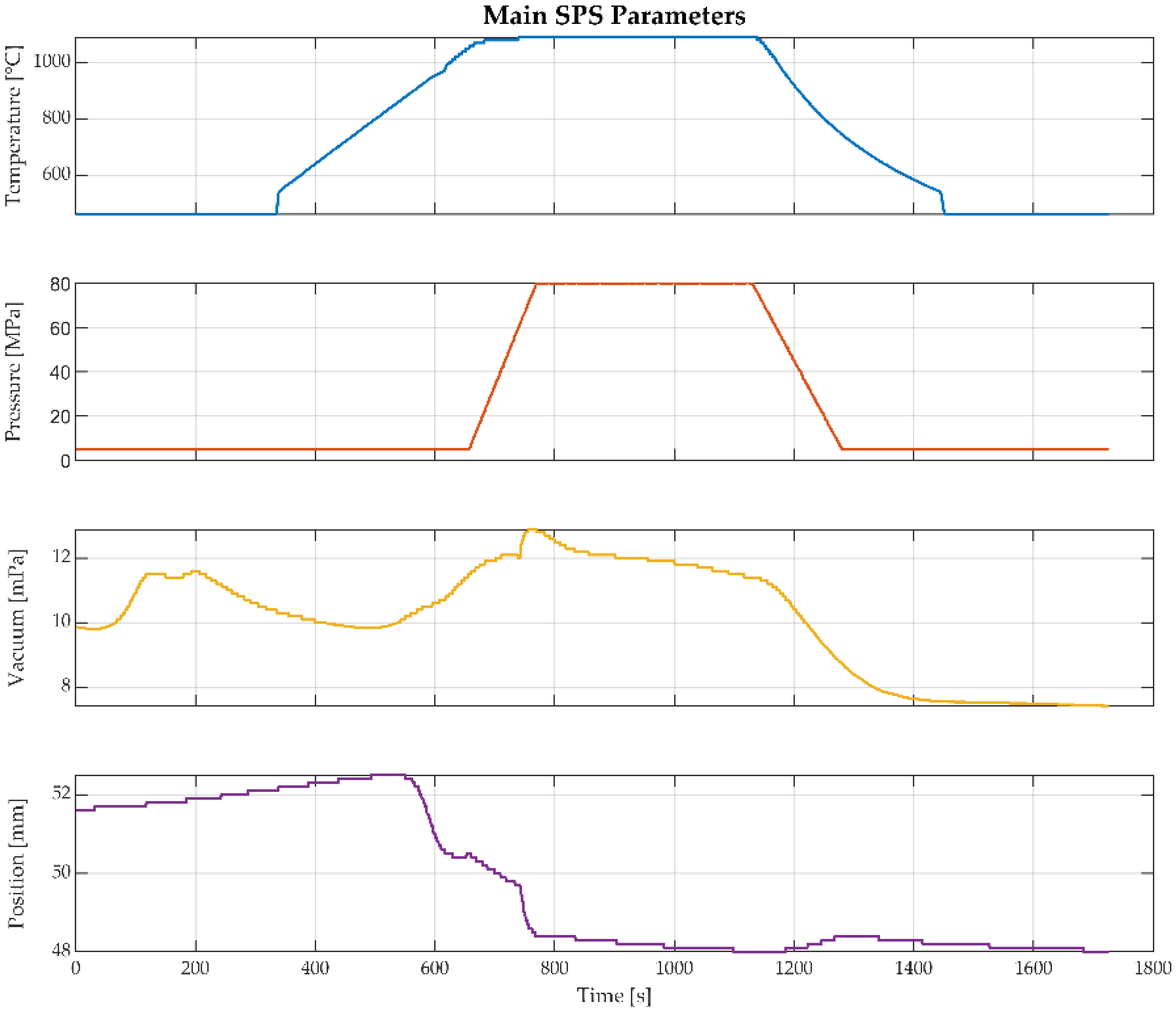
The evolution of the main SPS sintering parameters is displayed in Figure 2. The maximum pressure of 80 MPa was achieved at the moment of reaching the maximum temperature. The pressure in the chamber increased (i.e., vacuum loss) after the temperature reached about 800 °C, probably because of the air released from the gaps between particles at this temperature. The punch position is initially changing during heating, until about 900 °C, and then after the application of the pressure. The first decrease is caused by the initial movement of the particles in the powder. During and after the dwell time at the maximum temperature, the punch position was nearly constant. This is a sign of proper compaction conditions. In the HPF process, such in-situ monitoring is unfortunately not possible.
3.3. X-ray Diffraction of Fired Compacts
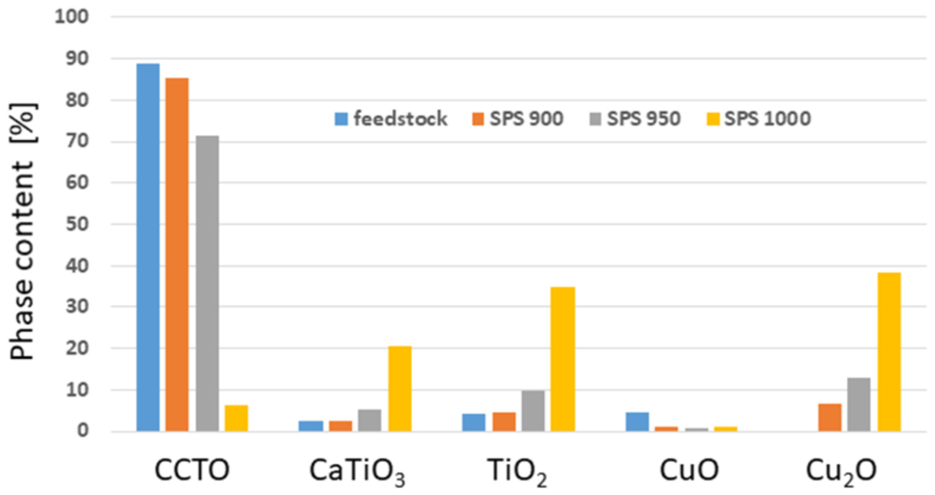
Figure 4 and Table 1 compares the phase contents in the as-fired samples obtained from the powder P2 sintered by SPS at various temperatures with other sintering conditions fixed. The dramatic fall of the CCTO content at 1000 °C is accompanied by an increase of the Cu2O amount. It has been reported that the presence of CuO (p-type semiconductor [21]) increases the high permittivity of the CCTO material, when is localized at the grain boundaries [1,3], while the presence of Cu2O, which is much more electrically conductive than CuO [3], is detrimental. Concerning the SPS of the powder P1, the problems related to the presence of Cu2O were similar or even worse.
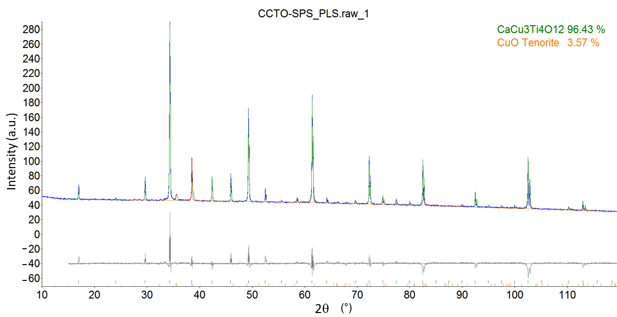
Figure 5 shows the XRD pattern of the pre-pressed HPF sample F sintered in a conventional furnace at 1050 °C. Besides the desired CCTO phase, it contained about 3.6% of CuO, which is probably advantageous; in fact, when it remains predominantly concentrated at the grain boundaries, it could contribute to the permittivity increase [11]. Table 2 compares phase analysis, lattice parameters and microhardness of our CCTO samples with those reported in other relevant studies. One can notice that the lattice parameter a of the CCTO structure in SPS sample D, containing a significant amount of Cu2O, is rather large, whereas other samples have similar lattice dimensions to those reported by other authors. The microhardness of sample D is rather high due to the presence of the Cu2O phase.
The samples O and R show CCTO single phase. Sample O was prepared by sol-gel [25], while sample R was synthesized by solid-state reaction using CaCO3, CuO and TiO2 precursors, followed by sintering for 12 h at 1050 °C [27]. Our powder P1 undergoes a partial decomposition during the SPS process that is accompanied by the appearance of Cu2O. This was one of the main disadvantages of SPS in combination with the powder produced using the NaCl-route. The key factor that allowed obtaining single phase in [25] and [27] is most likely related to the sintering in air. Sintering in an air-deficient environment, such as SPS, probably contributes to the pronounced chemical reduction of CuO to Cu2O. Our intention to use the SPS process for a fast production of CCTO dielectrics was limited by this aspect.
3.4. Microstructure
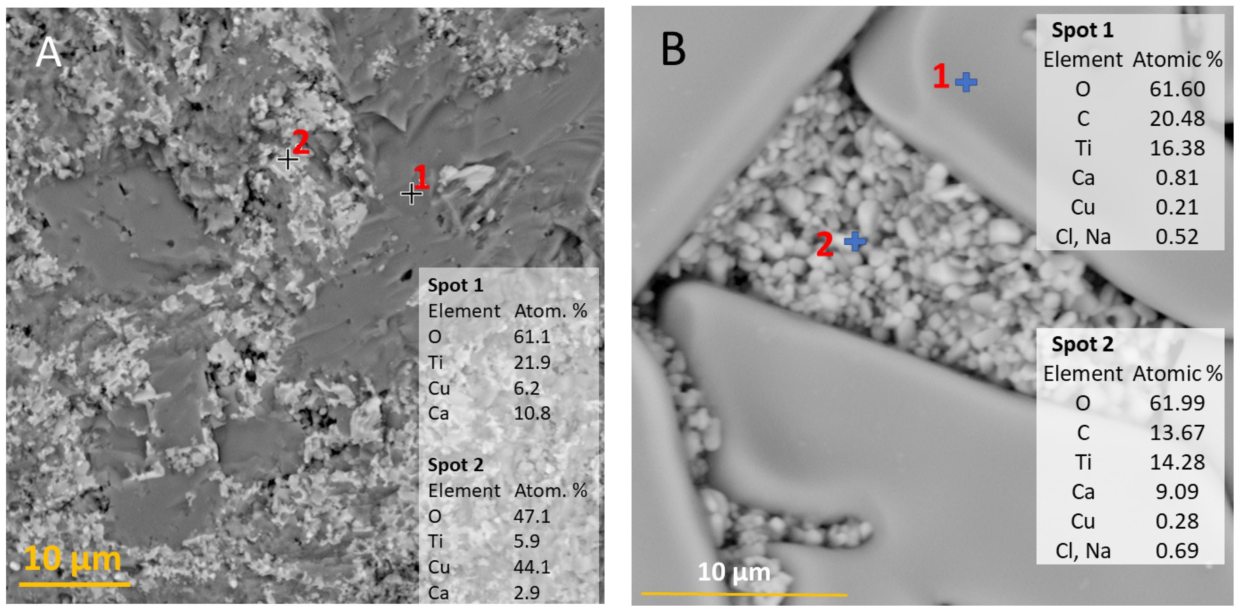
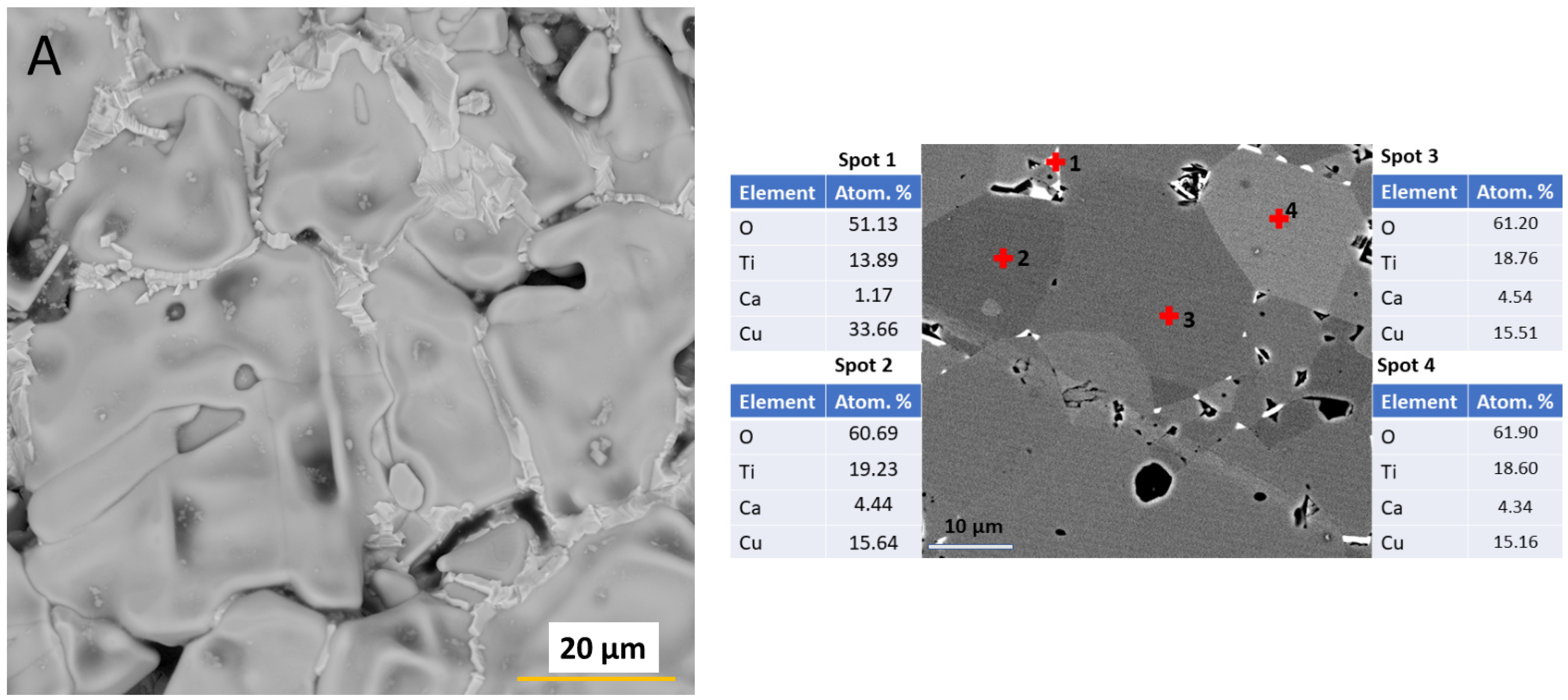
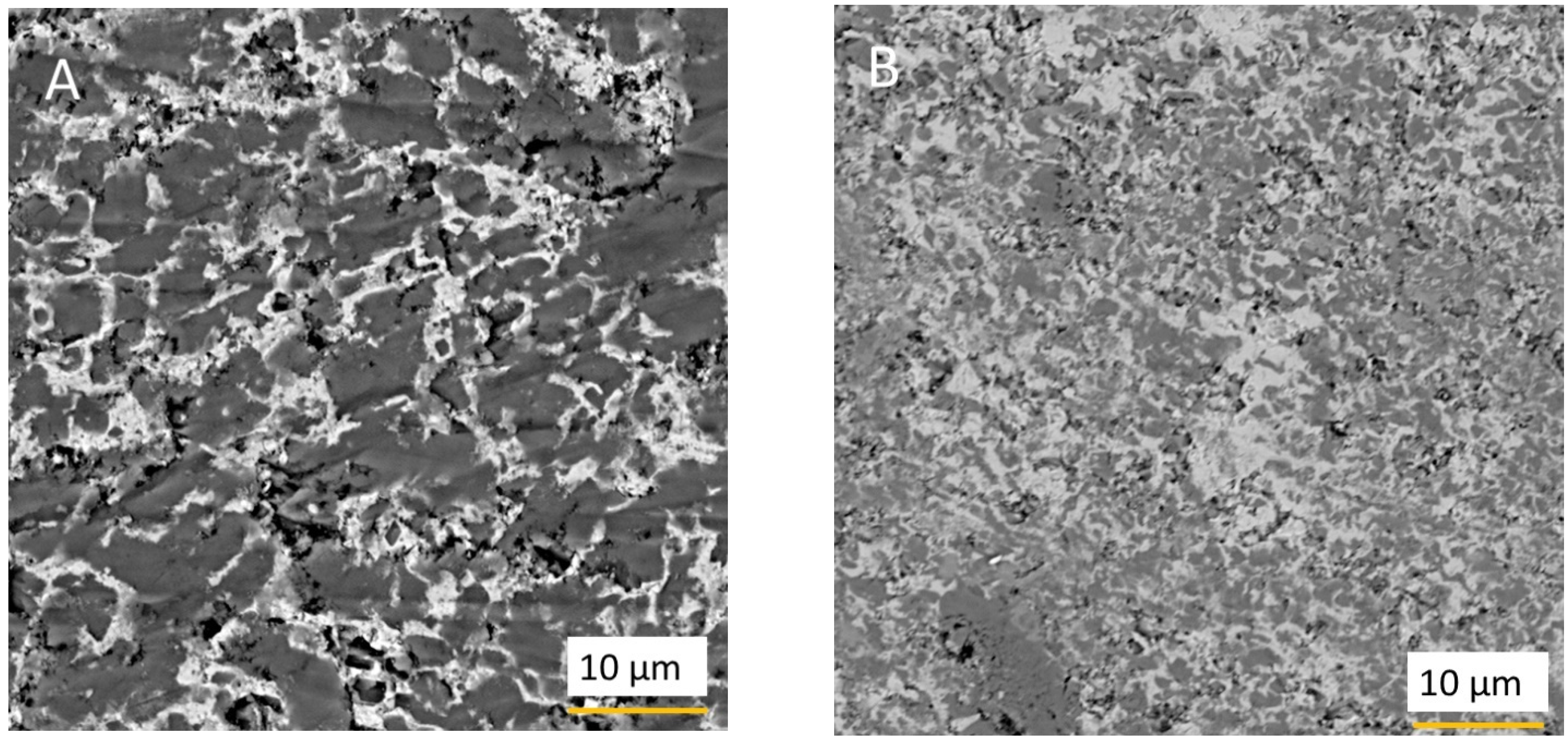
As Figure 6 displays, the microstructure of the CCTO materials fabricated by HPF and SPS is highly heterogeneous. The dark grey zones (Figure 6a, spot 1; sample F), and the light grey zones (Figure 6a, spot 2; sample F) represent areas rich in titanium and copper, respectively, while black areas correspond to pores. This is generally valid for all SPS and HPF samples. The white zones represent, however, the minority of the sample volume. Sample A seems to be rich in CaTiO3 and TiO2 (i.e., compounds with lower permittivity than CCTO). The distribution of Ca in sample A indicates that the important constituent of large grains is, besides the CCTO phase, probably TiO2, whereas in fine grains, besides the CCTO phase, the main phase is CaTiO3. Some carbon-containing phases are however present everywhere, c.f. the analysis in Figure 6b. The grains in the SPS samples appear similar to those observed in [32,33], showing a clear bimodal microstructure, with the finest and the coarsest grains differing by orders of magnitude (see for instance sample A in Figure 6b). In contrast, the microstructure of the samples fabricated by the HPF approach presents nearly-monomodal grains (see Figure 7 relative to sample I). The elemental analysis of sample E indicates that the white zones localized at grain boundaries are rich in copper with a content of about 33 at.% measured at location 1 (Figure 7b). These regions are most-likely corresponding to CuO. The Cu content in the grain interior is lower and it is about 15 at.% at locations 2 to 4 (see Figure 7b), despite subtle differences in the grey level. The typical characteristics of the microstructure of HPF samples consist of dark grains surrounded by a lighter matrix, with the latter being a contiguous phase, when the firing temperature is about 1050 °C (Figure 8a). When markedly lower cooling speed is applied, as in the case of HPF sample J (Figure 8b), even finer intermixing is present. Correspondingly, in references [9,25,34], a sintering temperature of 1050 °C is considered better than 1000 °C to reach good densification. The present results show that when the temperature is set to 1150 °C, the white-color components formed only thin shells around grains (see Figure 7).
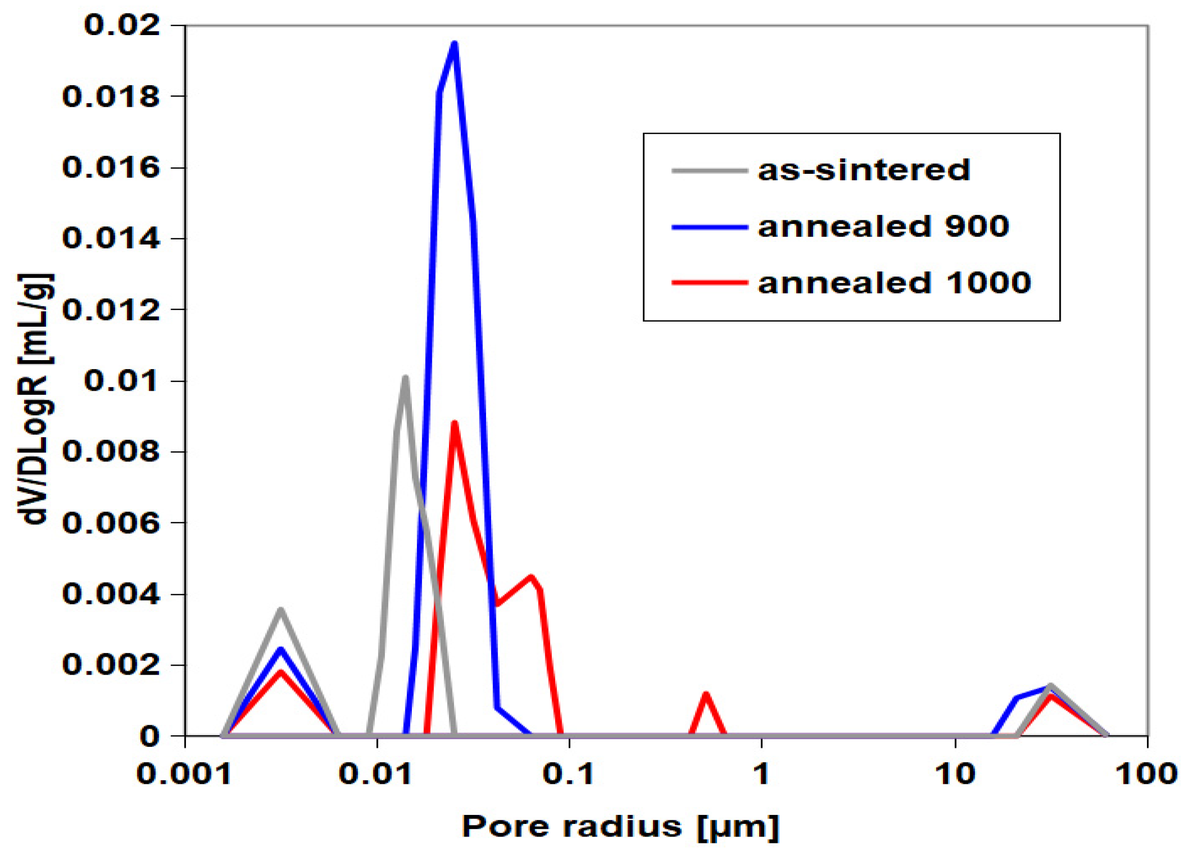
Figure 9 displays the mercury intrusion porosimetry (MIP) curves for the SPS sample A, which exhibited bimodal grain distribution in the as-sintered conditions. Considering the results and the change of porosity due to annealing, we can conclude that besides the above-mentioned separation of phases, annealing in air at about 1000 °C leads also to pores coalescence. The sample annealed at 900 °C presents a high peak at about 0.05 µm, while the sample annealed at 1000 °C presents two smaller peaks, one just below 0.1 µm and the other at about 0.7 µm, which is even smaller. This indicates that a process of pore coarsening occurred during annealing since the as-sintered sample shows a peak at about 0.01 µm. Pore coarsening is disadvantageous for improving the dielectric behavior. The small secondary peak around 50 µm corresponds to less-frequent coarse pores. Additionally, samples with bimodal grain size also tend towards bimodal porosity. It is possible that the annealing temperatures of 900 and 1000 °C were too high, since CCTO starts to sinter at about 850 °C. However, annealing at 850 °C was not sufficient to completely remove carbon contamination. Therefore, identifying the optimum annealing conditions is a challenging task and a compromise has to be found. The preliminary conclusion that could be drawn from these observations is that post-processing annealing treatment makes the production of SPS samples less economical and presents a low potential for improving the dielectric properties.
Additional porosity parameters for representatives of SPS and HPF samples are summarized in Table 3 with the exception that only the interval from 10 to 100 µm size shown in Figure 9 is included in Table 3. It can be noticed that the SPS sample is more porous than the HPF ceramic and contains flatter pores, i.e., with lower circularity, due to the application of pressure at hot conditions. The high porosity observed in the SPS sample A could be probably attributed to the lower homogeneity of powder P1. The presence of porosity in the SPS samples sintered from powder P2 is due to the presence of high melting point components (i.e., TiO2), which increase the temperature necessary to obtain high density. The good densification here attained by HPF is also supported by the Archimedean density of HPF sample E measured as 4.80 g/cm3, which corresponds to 0.1% open porosity.
The presence of CuO and Cu2O is responsible for the high micro-hardness of samples D and F, whose values around 16.5 GPa are close to those obtained in CuO-ZnO based materials reported in [35] and higher than the hardness of Cu2O [36]. On the other hand, it should be noticed that these residua are also responsible for the presence of fine pores, which are definitely undesired for the enhancement of the dielectric properties. Additionally, because of the Cu2O content, the SPS samples obtained from powder P1 are not promising dielectrics. However, these samples are rather interesting from the mechanical rigidity standpoint.
3.5. Electrical Properties
The comparison of sample A and sample B, both sintered by SPS under the same conditions using powder P1 and P2, respectively, allowed assessing the effect of the different powders on the electrical properties. Sample B had higher permittivity and higher resistivity, but also higher dielectric loss than sample A. None of these two samples exhibited a “giant permittivity”, and both show high dielectric loss, meaning that the processing conditions were non-optimal. Additionally, it was observed that annealing did not improve the microstructure of sample A, but instead, it led to pores coarsening. Since sample B showed improved dielectric properties compared to sample A, the powder P2 was used to prepare samples C and D, which enabled comparing the effect of the SPS sintering temperature. It could be noticed that an increase of the sintering temperature led to an increase of permittivity, but also to a simultaneous decrease of resistivity and CCTO phase content (see Table 2 and Table 4). Samples C and D were in fact a mixture of CCTO-CaTiO3-TiO2-CuO components, and although they might be regarded as new dielectrics, they still show dielectric loss tangent above 1. From the mechanical point of view, sample D showed high microhardness, but it was also brittle and presented handling problems, including cracking.
By comparing the samples sintered by the HPF approach using the powder P2 (samples G to J), one can notice that prolonging the dwell time led to slightly increased resistivity, but also to decreased permittivity and increased loss. Higher sintering temperature also decreased the permittivity. The same effect was also obtained using slower cooling (sample J). The present comparison allowed identifying the optimum processing conditions for powder P2: HPF, sintering temperature from 1100 °C to 1150 °C, dwell time of 2 h, identical heating and cooling rate of 7 °C /min.
Table 4 also provides a comparison of the dielectric properties and resistivity with typical values reported in the literature. The combination of a relative permittivity over 20,000 with a loss tangent of around 0.1 in the whole frequency range is rare and represents an attractive attribute of some of our samples, i.e., sample I. While some of the samples show remarkable relative permittivity values, e.g., G, H and J, it should be noticed that there is a considerable increase of the loss tangent values at higher frequencies. Therefore, we can consider that our sample I presents the optimal balance of both quantities–permittivity and losses. An interesting balance in dielectric properties is also found in the samples tested by Jesus et al. [37] that show a relative permittivity of 21,000 and loss tangent of 0.2 at 10 kHz.
In the consulted literature, two rather opposite trends in the dielectric properties have been identified. The first trend is displayed by materials with a giant permittivity, i.e., 100,000 or higher, accompanied by rather high loss tangent values (over 1) [24]. A long dwell time of 12 h at the sintering temperatures of 1050 °C and 1100 °C [24] seems to be the reason behind this behavior. The second trend is characterized by a reasonably low loss tangent, i.e., less than 0.2 [22], typically accompanied by low permittivity values of around 1000, for frequencies lower than 1 kHz. The fast processing method of SPS seems to determine the second type of trend, as demonstrated by our SPS sample C, c.f. Table 4. Values of permittivity and losses between the mentioned edges are shown by sample M [36]. An interesting comparison between our HPF samples and those reported in the literature could be made referring again to the work by Liu et al. [24], who demonstrated that a change in the firing temperature from 1050 °C to 1100 °C strongly affects the dielectric response. In particular, samples sintered at 1050 °C/8 h and 1050 °C/12 h showed higher permittivity and lower losses than those fabricated at 1100 °C/12 h, and 1050 °C/4 h [24]. In our work, the HPF samples sintered in air were fired at 1100 °C and 1150 °C for much shorter dwell times (typically one or two hours), and showed combinations of εr over 30,000 and Tan δ below 0.1 at 1 kHz.
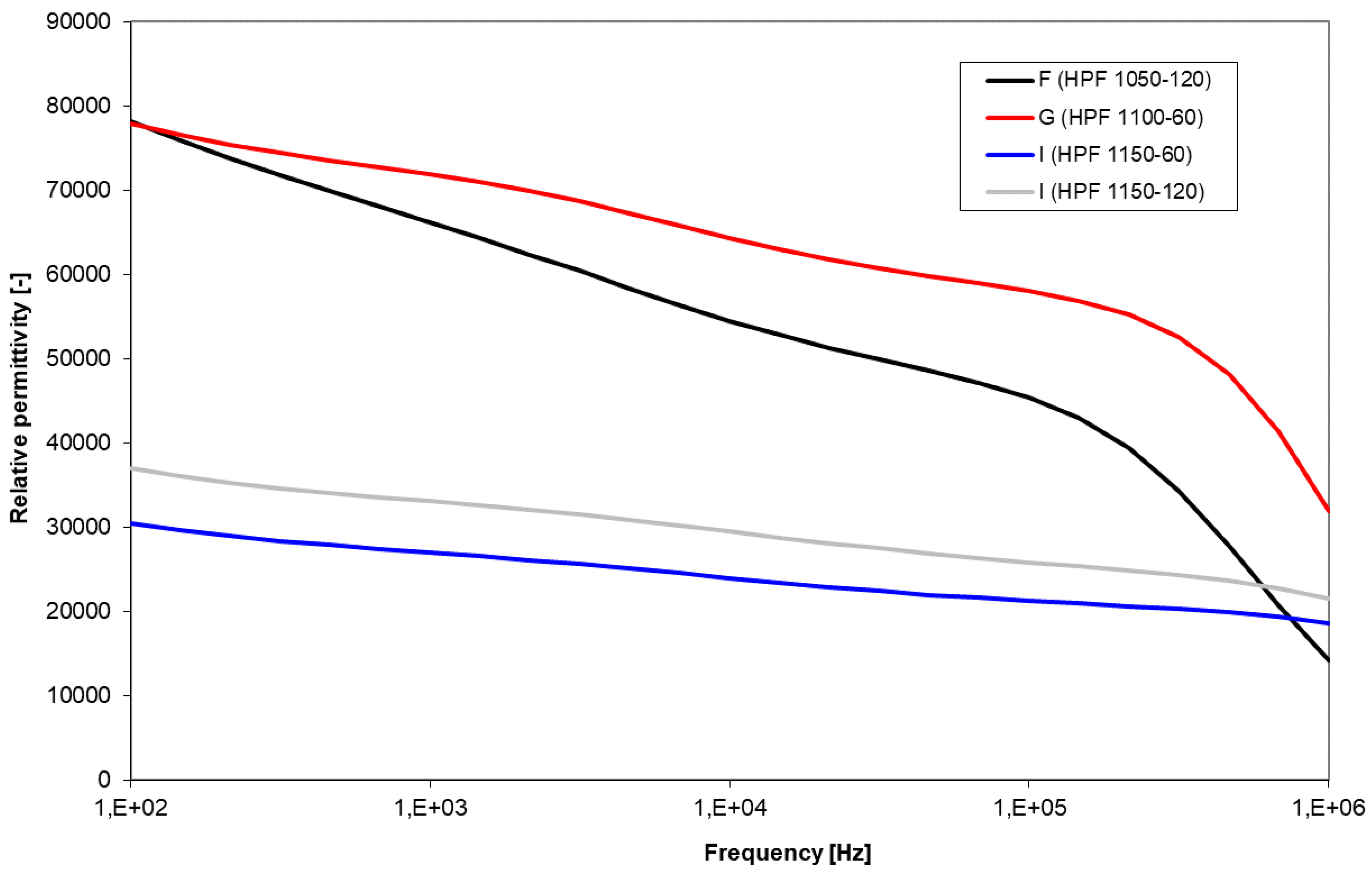
Regarding the frequency dependence of the dielectric properties of CCTO ceramics, it can be observed that, in general, the relative permittivity is lower at high frequency, as usually occurs in dielectrics due to the decreasing number of polarization mechanisms remaining active with increasing frequency. Concerning the dependence of the loss tangent of CCTO on the frequency, two types of trends can be identified in Table 4: (a) the loss tangent increases with frequency, as shown by our samples G, H, J and K fired at temperatures below 1150 °C, and by samples M [23], O [25], S [28], T [29], U [30], from the literature; (b) the loss tangent decreases with frequency, as observed in our samples B, C, D, and partly by the laser-sintered CCTO samples reported in [24].
Figure 10 and Figure 11 display the frequency dependence of permittivity and loss tangent of selected HPF samples at room temperature. The samples fired below 1150 °C (samples F and G) show the behavior previously indicated as (a), which is promising for low-frequency applications. The samples fired at 1150 °C remain more stable with changing frequency. Compared to the long dwell times often reported in the literature (even 48 h in some cases [29]), our HPF samples are prepared with a relatively short sintering time, which validates our efforts to fabricate good-quality dielectrics with rather low thermal energy input.
Concerning the chemical composition and phase composition of CCTO, it seems that neither phase purity nor stoichiometry can be directly linked to the trends observed in the loss tangent. Therefore, other mechanisms should be sought.
In the attempt to relate the effect of the microstructure on the dielectric properties, it can be recalled that the dielectric response of CCTO is also affected by the presence of space charge in nanosize volumes [38, 39], often located around planar defects, such as those designated as polaronic stacking faults in the defect model proposed by Bueno et al. [26]. In the latter, it was proposed that the stacking faults present at the nanoscale work as a large assemble of internal barrier layer capacitors, thus resulting in the giant relative permittivity ε′ observed in CCTO-based materials. This phenomenon is referred to as nanoscale barrier layer capacitance (NBLC) and leads to a marked enhancement of polaronic defects. According to Ribeiro et al. [40], also the Debye relaxation process exhibited by polycrystalline CCTO samples at high frequency is based on polaronic defects. Additionally, the presence of NBLC was discussed as a condition for preserving the giant permittivity up to MHz frequency range, whereas the only presence of the microscale MBLC effects should be responsible for the permittivity relaxation and the increase of loss tangent in the kHz range, indicated above as trend (a). According to the study by Ivanov et al. [9], the MBLC and NBLC frames in CCTO reach sizes above 5 µm and 200 nm, respectively. These features have been most likely observed also in the work of Lin et al. [41], possibly corresponding to the dark submicrometric dots displayed in the SEM micrographs, although these have not been linked to NBLC. According to our assumption, the MBLC size range corresponds to the “grain size range”, of few micrometers. The dependence of dielectric properties on grain size is clearly visible at low frequencies. Similarly, crystallites, as half-order of magnitude smaller objects than grains, are probably more influential on the dielectric behavior at much higher frequencies. According to our opinion, the size of NBLC zones corresponds to the crystallites size. This is also supported by the analysis carried out by Ivanov et al. [9]. They showed that the total impedance of 300 GΩ in so-called Nyquist plot can be decomposed into the contributions of various-scale components, obtaining ZMBLC = 10 GΩ, ZNBLC1 = 40 GΩ and ZNBLC2 = 250 GΩ. In particular, ZNBLC1 is related to microstructural features exhibiting a terrace-ledge morphology associated with the spiral growth of crystals via a screw dislocation [9], whereas ZNBLC2 is linked to more isotropic mesh-like morphology. This “mesh” is the standard structure of ultra-fine grains and grain boundaries, which are about 100 nm thick [9]. According to our assumptions, crystallite boundaries correspond to the nanoscale barriers, while grain boundaries to the microscale barriers.
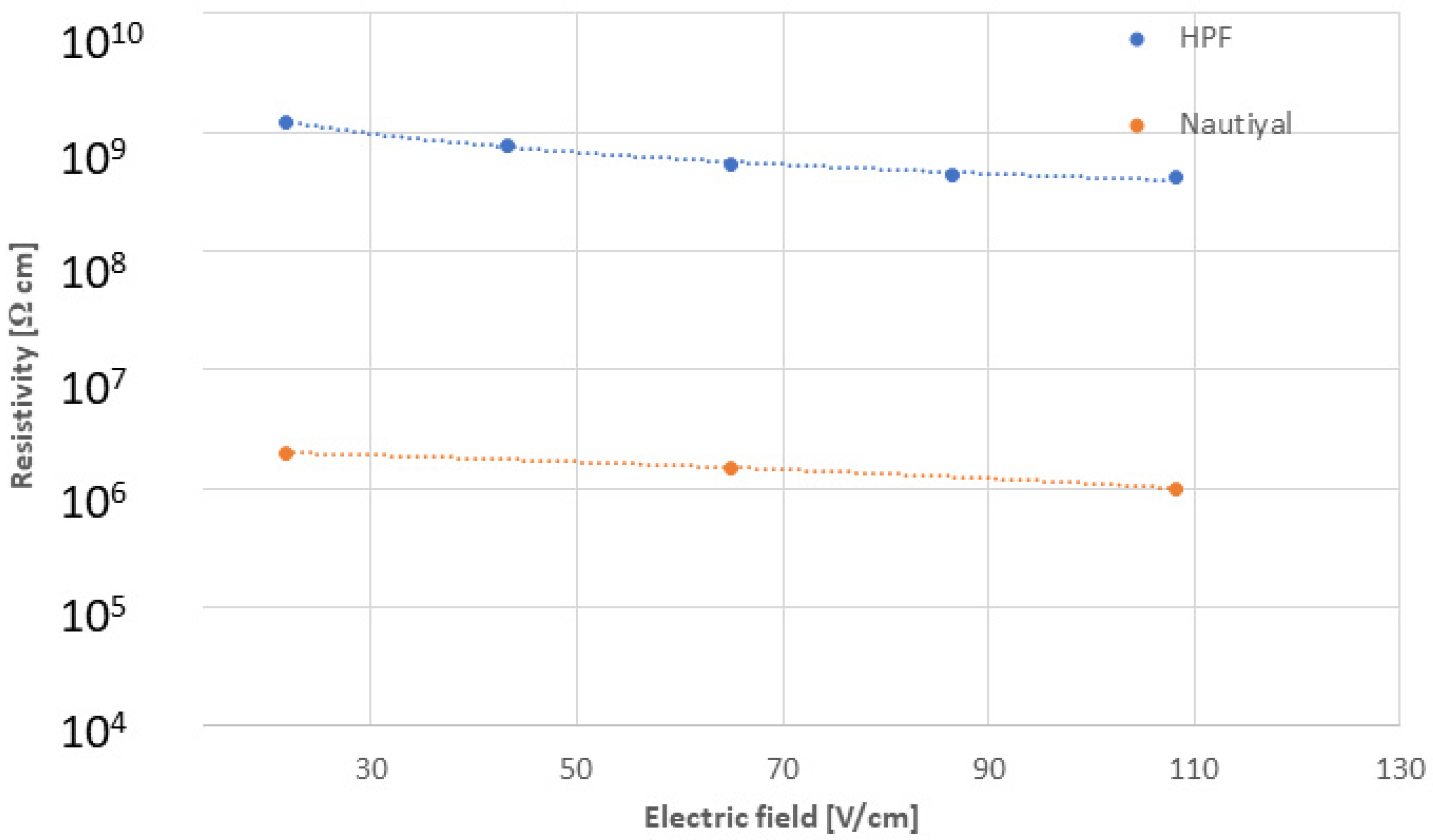
The DC volume resistivity ρv is not particularly suitable for distinguishing high-quality samples. We could just summarize that high-permittivity samples had resistivity in the order of magnitude 106 Ωm, c.f. Table 4. However, sometimes higher values around 107 Ωm have been reported [25]. Unfortunately, due to the lack of data simultaneously reporting phase composition and resistivity in the literature, a clear relationship between the CCTO phase content and resistivity cannot be established. Figure 12 shows the dependence of the DC resistivity on the intensity of the applied electric field for our sample I (highest resistivity of our HPF samples), in comparison with the data published by Nautiyal et al. for sol-gel synthesized CCTO [23]. In both cases, the resistivity decreases by about half order of magnitude between 25 and 105 V/cm bias electric field intensity. From this standpoint, CCTO is much less stable compared to conventional perovskite dielectrics like CaTiO3 [42].
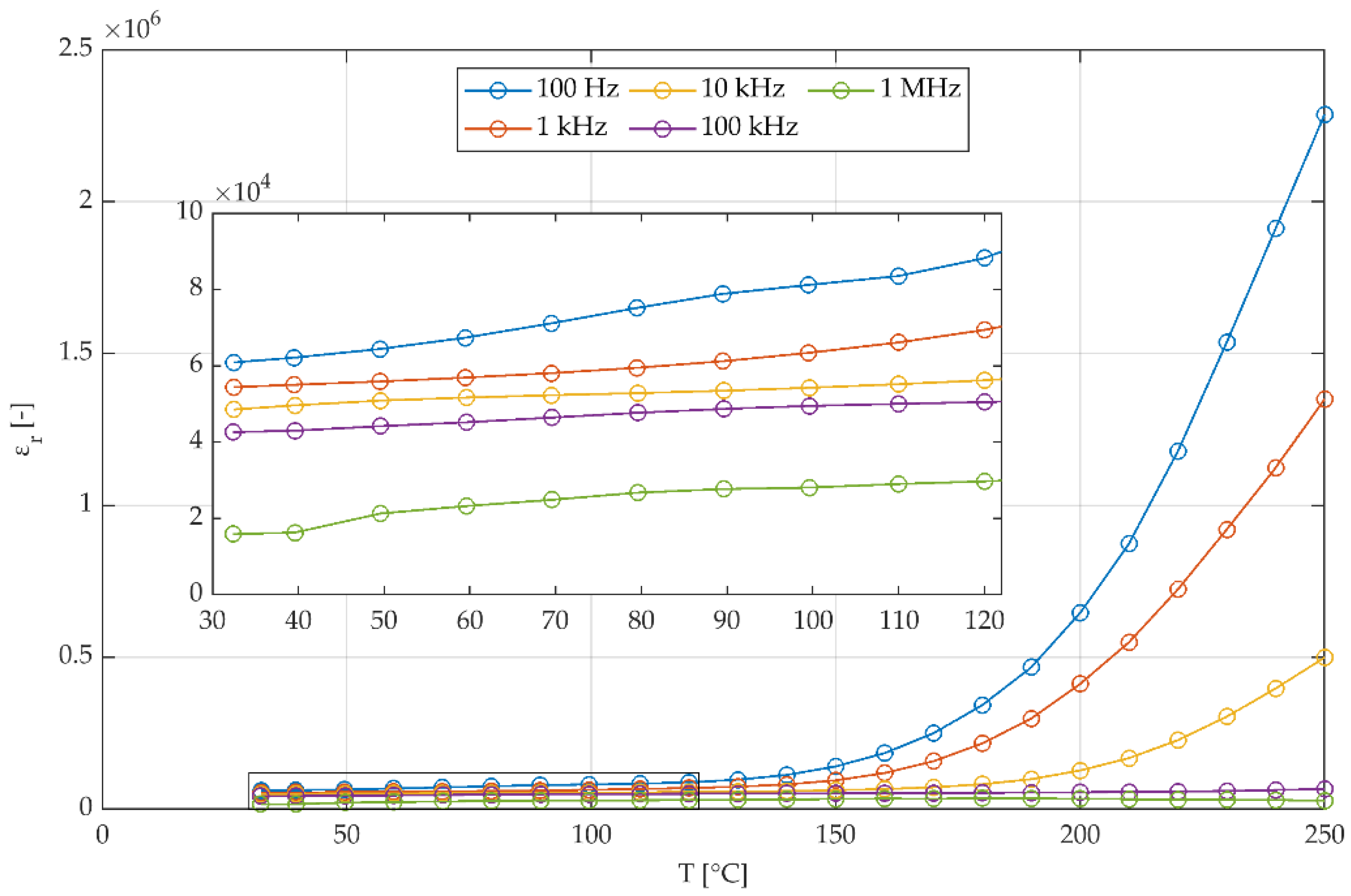
Figure 13 shows the temperature dependence of the permittivity up to 250 °C for different frequencies in the range 100 Hz-1 MHz. It can be noticed that, as expected, the relative permittivity increases at low frequency and high temperature. The significant variation of the permittivity with temperature for 100 Hz and 1 kHz frequency is associated with space-charge polarization [3]. However, a large response of CCTO to a rather small change in frequency and temperature could be advantageous for designing a sensor for applications above 200 °C and below 1 kHz. At frequencies in the kHz range, the permittivity is rather stable up to about 120 °C, as shown in the inset graph.
4. Conclusions
In relation to the initial goals of the present work, the following conclusions can be drawn.
Goal 1-To synthesize the feedstock powder via the molten salt route.
The molten salt synthesis process was successful in obtaining powder P1 with a CCTO percentage of over 80%, but with the presence of CaTiO3, TiO2 and CuO as secondary phases and small residues of NaCl. The commercial powder P2 also contained impurities, such as CaTiO3, TiO2 and CuO. The powder P1 could be sintered by SPS starting from 900 °C, while for powder P2, the SPS sintering temperature had to be increased to 950 °C and even 1000 °C for better densification. The higher TiO2 content seems to be the factor responsible for the shift of the sintering onset to higher temperatures. The commercial powder P2 led to higher success in forming the CCTO phase, especially under oxidative conditions during HPF processing, thanks to the absence of residual NaCl and better uniformity of particle sizes and shapes.
Goal 2-To compare the use of the SPS process and the SPS-related modification of a conventional sintering process (labeled HPF) on the microstructure of CCTO compacts.
The reducing conditions during SPS favored the formation of CuO and Cu2O, especially using the powder P1. These phases are mechanically hard but brittle. The samples fabricated by SPS with the commercial powder P2 showed lower Cu2O content and more homogeneous microstructures compared to the SPS samples obtained from powder P1 sintered under the same conditions. However, all SPS samples exhibited pronounced grain size bimodality. Pore coarsening, which is disadvantageous for improving the dielectric behavior, was observed in SPS samples after annealing. The HPF technique is advantageous for its non-reducing atmosphere. The HPF samples sintered using both powders typically present lower porosity and lower grain size bimodality than those found in SPS samples.
Goal 3-To compare the dielectric properties of the fired bulks obtained from different powders sintered by different methods.
In the case of SPS samples, regardless of the powder used, giant permittivity could not be achieved, and a rather fast decrease in permittivity was observed with increasing frequency. The conductance component of the permittivity, probably caused by the free electrons in the Cu2O phase, is probably responsible for this phenomenon. Consequently, dielectric losses were also rather high. Concerning the fabrication of suitable CCTO dielectrics using the HPF approach, we can conclude that the sintering temperature should be set over 1100 °C. The optimum HPF sintering temperature for the commercial powder P2 was identified as 1150 °C, partly because of the high TiO2 content. Microstructural factors, such as low porosity and low grain size bimodality, governed the improved dielectric behavior of the HPF samples compared to those prepared by SPS. The capacitance component of the permittivity manifested space-charge polarization mechanisms, i.e., increased permittivity just at very low frequencies. The best samples among those fabricated by HPF exhibited high relative permittivity, while maintaining rather low losses, with values generally comparable to the best achievements reported in the literature. The relative permittivity of these samples remained over 50,000 up to the frequency of 200 kHz at room temperature. For f < 200 kHz, their capacitance did not show space-charge polarization mechanisms, as evidenced by the weak dependence of the loss tangent on the frequency. So far, these features are among the best achievements obtained in CCTO ceramics because the permittivity remained high and the loss tangent low in a rather broad frequency range. Moreover, this holds not only near room temperature but also up to about 200 °C. On the other hand, the DC resistivity of CCTO remained rather voltage-dependent. The HPF firing times necessary for producing these dielectrics were not longer than two hours, achieving the initial objective of reducing the thermal load during processing.
A possibly viable way to prepare very high-quality CCTO ceramics is to combine the HPF approach with longer firing dwell times. This is an interesting task for subsequent investigations. In the search for the optimum dwell time, various parameters such as density, grain size and copper oxide distribution should be carefully evaluated and optimized.
Author Contributions
J.P. experimentation–powder synthesis, dielectric measurements; P.C. experimentation–sintering, test evaluations, manuscript draft writing; J.S. experimentation–metal contacts design and fabrication, consultations; F.L. experimentation–XRD analyses and interpretation. All authors have read and agreed to the published version of the manuscript.
Funding
This research was supported by the Grant Agency of the Czech Technical University in Prague, No. SGS21/058/OHK3/1T/13.
Institutional Review Board Statement
Not applicable.
Informed Consent Statement
Informed consent was obtained from all subjects involved in the study.
Acknowledgments
The authors would like to thank to SEM operator Petr Veselý, FEE CTU Prague.
Conflicts of Interest
The author declares no conflict of interest.
References
- Almeida, A.F.L.; Oliveira, R.S.; Goes, J.C.; Sasaki, J.M.; Souza, F.A.G.; Mendes, F.J.; Sombra, A.S.B. Structural Properties of CaCu3Ti4O12 Obtained by Mechanical Alloying. Mat. Sci. Eng. B 2002, 96, 275–283. [Google Scholar] [CrossRef]
- Valim, D.; Filho, A.G.S.; Freire, P.T.C.; Fagan, S.B.; Ayala, A.P.; Filho, J.M.; Almeida, A.F.L.; Fechine, P.B.A.; Sombra, A.S.B.; Olsen, J.S.; et al. Raman Scattering and X-ray Diffraction Studies of Polycrystalline CaCu3Ti4O12 Under High-pressure. Phys. Rev. B 2004, 70, 132103. [Google Scholar] [CrossRef] [Green Version]
- Shan, X. High Dielectric Constant Ceramic-Polymer Composites. Ph.D. Thesis, Auburn University, Auburn, AL, USA, 2009. [Google Scholar]
- Wu, L.; Zhu, Y.; Park, S.; Shapiro, S.; Shirane, G. Defect Structure of the High-Dielectric Constant Perovskite CaCu3Ti4O12. Phys. Rev. B 2005, 71, 014118. [Google Scholar] [CrossRef] [Green Version]
- Cohen, M.H.; Neaton, J.B.; Lixin, H.; Vanderbilt, D. Extrinsic Models for the Dielectric Response of CaCu3Ti4O12. J. Appl. Phys. 2003, 94, 3299–3306. [Google Scholar] [CrossRef] [Green Version]
- Krohns, S.; Lunkenheimer, P.; Ebbinghaus, S.G.; Loidl, A. Colossal Dielectric Constants in Single-crystalline and Ceramic CaCu3Ti4O12 Investigated by Broadband Dielectric Spectroscopy. J. Appl. Phys. 2008, 103, 084107. [Google Scholar] [CrossRef]
- Subramanian, M.A.; Li, D.; Duan, N.; Reisner, B.A.; Sleight, A.W. High Dielectric Constant in ACu3Ti4O12 and ACu3Ti3FeO12 Phases. J. Solid State Chem. 2000, 151, 323–325. [Google Scholar] [CrossRef]
- Subramanian, M.A.; Sleight, A.W. Cu3Ti4O12 and Cu3Ru4O12 Perovskites: High Dielectric Constants and Valence Degeneracy. Solid State Sci. 2002, 4, 347–351. [Google Scholar] [CrossRef]
- Ivanov, M.S.; Amaral, F.; Khomchenko, V.A.; Paixão, J.A.; Costa, L.C. Investigation of Micro and Nanoscale Barrier Layer Capacitance Mechanisms of Conductivity in CaCu3Ti4O12 Via Scanning Probe Microscopy Technique. RSC Adv. 2017, 7, 40695–40704. [Google Scholar] [CrossRef] [Green Version]
- Wang, C.C.; Zhang, L.W. Oxygen-vacancy-related Dielectric Anomaly in CaCu3Ti4O12: Post-sintering Annealing Studies. Phys. Rev. B 2006, 74, 024106. [Google Scholar] [CrossRef]
- Schmidt, R.; Pandey, S.; Fiorenza, P.; Sinclair, D.C. Non-stoichiometry in CaCu3Ti4O12 (CCTO) Ceramics. RSC Adv. 2013, 3, 14580–14589. [Google Scholar] [CrossRef] [Green Version]
- Yoon, S.; Dornseiffer, J.; Xiong, Y.; Grüner, D.; Shen, Z.; Iwaya, S.; Pithan, C.; Waser, R. Spark Plasma Sintering of Nanocrystalline BaTiO3 powders: Consolidation Behavior and Dielectric Characteristics. J. Eur. Ceram. Soc. 2011, 31, 1723–1731. [Google Scholar] [CrossRef]
- Su, B.; He, J.Y.; Cheng, B.L.; Button, T.W.; Liu, J.; Shen, Z.; Nygren, M. Dielectric Properties of Spark Plasma Sintered (SPS) Barium Strontium Titanate (BST) Ceramics. Integr. Ferroelectr. An. Int. J. 2004, 61, 74–81. [Google Scholar] [CrossRef]
- Ctibor, P.; Kubatík, T.; Chráska, P. Spark Plasma Sintering of Multilayer Ceramics–Case Study of Al2O3–Mg(Ca)TiO3 Sandwich. Key Eng. Mater. 2014, 606, 205–208. [Google Scholar] [CrossRef]
- Herrera Robles, J.O.; Rodriguez Gonzalez, C.A.; Diaz de la Torre, S.; Fuentes Cobas, L.E.; Garcia Casillas, P.E.; Camacho Montes, H. Dielectric Properties of Bismuth Titanate Densified by Spark Plasma Sintering and Pressureless Sintering. J. Alloys Compd. 2012, 536S, S511–S515. [Google Scholar] [CrossRef]
- Anselmi-Tamburini, U.; Garay, J.E.; Munir, Z.A. Fast Low-temperature Consolidation of Bulk Nanometric Ceramic Materials. Scr. Mater. 2006, 54, 823–828. [Google Scholar] [CrossRef]
- Wan, W.; Yang, J.; Yuan, W.; Zhao, X.; Liu, C.; Qiu, T. Preparation of Giant Dielectric CaCu3Ti4O12 Ceramics via the Molten Salt Method from NaCl Flux. Int. J. Appl. Ceram. Technol. 2016, 13, 382–388. [Google Scholar] [CrossRef]
- Rietveld, H.M. A Profile Refinement Method for Nuclear and Magnetic Structures. J. Appl. Crystallogr. 1969, 2, 65–71. [Google Scholar] [CrossRef]
- Rietveld, H.M. Line Profiles of Neutron Powder-diffraction Peaks for Structure Refinement. Acta Crystallogr. 1967, 22, 151–152. [Google Scholar] [CrossRef]
- Cheary, R.W.; Coelho, A. A Fundamental Parameters Approach to X-ray Line-profile Fitting. J. Appl. Crystallogr. 1992, 25, 109–121. [Google Scholar] [CrossRef]
- Kawrani, S.; Boulos, M.; Bekheet, M.F.; Viter, R.; Nada, A.A.; Riedel, W.; Roualdes, S.; Cornu, D.; Bechelany, M. Segregation of Copper Oxide on Calcium Copper Titanate Surface Induced by Graphene Oxide for Water Splitting Aapplications. Appl. Surf. Sci. 2020, 516, 146051. [Google Scholar] [CrossRef]
- Manière, C.; Riquet, G.; Marinel, S. Dielectric Properties of Flash Spark Plasma Sintered BaTiO3 and CaCu3Ti4O12. Scr. Mater. 2019, 173, 41–45. [Google Scholar] [CrossRef]
- Nautiyal, A.; Autret, C.; Honstettre, C.; Didry, S.; El Amrani, M.; Roger, S.; Ruyter, A. Dielectric Properties of CCTO/MgTiO3 Composites: A New Approach for Capacitor Application. Int. J. Adv. Nanomater. 2015, 1, 27–40. [Google Scholar]
- Liu, P.; Lai, Y.; Zeng, Y.; Wu, S.; Huang, Z.; Han, J. Influence of Sintering Conditions on Microstructure and Electrical Properties of CaCu3Ti4O12 (CCTO) Ceramics. J. Alloys Compd. 2015, 650, 59–64. [Google Scholar] [CrossRef]
- Chiodelli, G.; Massarotti, V.; Capsoni, D.; Bini, M.; Azzoni, C.B.; Mozzati, M.C.; Lupotto, P. Electric and Dielectric Properties of Pure and Doped CaCu3Ti4O12 Perovskite Materials. Solid State Commun. 2004, 13, 241–246. [Google Scholar] [CrossRef]
- Bueno, P.R.; Tararan, R.; Parra, R.; Joanni, E.; Ramírez, M.A.; Ribeiro, W.C. A polaronic Stacking Fault Defect Model for CaCu3-Ti4O12 Material: An Approach for the Origin of the Huge Dielectric Constant and Semiconducting Coexistent Features. J. Phys. D Appl. Phys. 2009, 42, 055404. [Google Scholar] [CrossRef] [Green Version]
- Orrego, S.; Cortés, J.A.; Amoresi, R.A.C.; Simões, A.Z.; Ramírez, M.A. Photoluminescence Behavior on Sr2+ Modified CaCu3Ti4O12 Based Ceramics. Ceram. Int. 2018, 44, 10781–10789. [Google Scholar] [CrossRef] [Green Version]
- Gelfuso, M.V.; Montoya Uribe, J.O.; Thomazini, D. Deficient or Excessive CuO-TiO2 Phase Influence on Dielectric Properties of CaCu3Ti4O12 Ceramics. Int. J. Appl. Ceram. Technol. 2019, 16, 868–882. [Google Scholar] [CrossRef]
- Sun, Y. Dielectric Properties of CaCu3Ti4O12 and Its Related Materials. Ph.D. Thesis, University of Arkon, Akron, OH, USA, 2006. [Google Scholar]
- Li, W.; Tang, L.; Xue, F. Large Reduction of Dielectric Losses of CaCu3Ti4O12 Ceramics Via Air Quenching. Ceram. Int. 2017, 43, 6618–6621. [Google Scholar] [CrossRef]
- Ramírez, M.A.; Parra, R.; Reboredo, M.M.; Varela, J.A.; Castro, M.S.; Ramajo, L. Elastic Modulus and Hardness of CaTiO3, CaCu3Ti4O12 and CaTiO3/CaCu3Ti4O12 Mixture. Mater. Lett. 2010, 64, 1226–1228. [Google Scholar] [CrossRef]
- Mao, P.; Wang, J.; Liu, S.; Zhang, L.; Zhao, Y.; Mao, L.H. Grain Size Effect on the Dielectric and Non-ohmic Properties of CaCu3Ti4O12 Ceramics Prepared by the Sol-gel Process. J. Alloys Compd. 2019, 778, 625–632. [Google Scholar] [CrossRef]
- Guillemet-Fritsch, S.; Lebey, T.; Boulos, M.; Durand, B. Dielectric Properties of CaCu3Ti4O12 Based Multiphased Ceramics. J. Eur. Ceram. Soc. 2006, 26, 1245–1257. [Google Scholar] [CrossRef] [Green Version]
- Mohamed, J.J.; Hutagalung, S.D.; Ahmad, Z.A. Influence of sintering parameters on melting CuO phase in CaCu3Ti4O12. J. King Saud Univ. Eng. Sci. 2013, 25, 35–39. [Google Scholar] [CrossRef] [Green Version]
- Susilawati, T.; Nasution, I.; Hasanah, M.; Sihombing, Y.A. Fabrication of Ceramic Composites Based on CuO-ZnO. J. Phys. Conf. Ser. 2018, 1116, 032038. [Google Scholar] [CrossRef]
- Jian, S.-R.; Chen, G.-J.; Hsu, W.-M. Mechanical Properties of Cu2O Thin Films by Nanoindentation. Materials 2013, 6, 4505–4513. [Google Scholar] [CrossRef] [PubMed] [Green Version]
- Jesus, L.M.; Santos, J.C.A.; Sampaio, D.V.; Barbosa, L.B.; Silva, R.S.; M’Peko, J.-C. Polymeric Synthesis and Conventional Versus Laser Sintering of CaCu3Ti4O12 Electroceramics: (Micro)structures, Phase Development and Dielectric Properties. J. Alloys Compd. 2016, 654, 482–490. [Google Scholar] [CrossRef]
- Lunkenheimer, P.; Fichtl, R.; Ebbinghaus, S.G.; Loidl, A. Nonintrinsic Origin of the Colossal Dielectric Constants in CaCu3Ti4O12. Phys Rev. B 2004, 70, 172102. [Google Scholar] [CrossRef] [Green Version]
- Ahmadipour, M.; Ain, M.F.; Ahmad, Z.A. A Short Review on Copper Calcium Titanate (CCTO) Electroceramic: Synthesis, Dielectric Properties, Film Deposition, and Sensing Application. Nano-Micro Lett. 2016, 8, 291–311. [Google Scholar] [CrossRef] [Green Version]
- Ribeiro, W.C.; Joanni, E.; Savu, R.; Bueno, P.R. Nanoscale Effects and Polaronic Relaxation in CaCu3Ti4O12 Compounds. Solid State Commun. 2011, 151, 173–176. [Google Scholar] [CrossRef] [Green Version]
- Lin, H.; He, X.; Gong, Y.; Pang, D.; Yi, Z. Tuning the Nonlinear Current-voltage Behavior of CaCu3Ti4O12 Ceramics by Spark Plasma Sintering. Ceram. Int. 2018, 44, 8650–8655. [Google Scholar] [CrossRef]
- Sedláček, J.; Ctibor, P.; Kotlan, J.; Pala, Z. Dielectric properties of CaTiO3 coatings prepared by plasma spraying. Surf. Eng. 2013, 5, 384–389. [Google Scholar] [CrossRef]
Figure 1.
XRD patterns of P1 powder produced using the molten salt route and P2 commercial powder. Grey color indicates the “difference between fit and model”.
Figure 1.
XRD patterns of P1 powder produced using the molten salt route and P2 commercial powder. Grey color indicates the “difference between fit and model”.

Figure 2.
Typical evolution of main SPS parameters during processing.

Figure 3.
Scheme of the experiments. Steps applicable at the same time are in the same horizontal level.
Figure 3.
Scheme of the experiments. Steps applicable at the same time are in the same horizontal level.

Figure 4.
Phase content [%] in the SPS samples B, C, D (see Table 1) sintered at 900, 950, and 1000 °C from the P2 powder.
Figure 4.
Phase content [%] in the SPS samples B, C, D (see Table 1) sintered at 900, 950, and 1000 °C from the P2 powder.

Figure 5.
XRD analysis of sample F (see Table 1) fired at 1050 °C for 2 h from the P2 powder. Grey color indicates the “difference between fit and model”.
Figure 5.
XRD analysis of sample F (see Table 1) fired at 1050 °C for 2 h from the P2 powder. Grey color indicates the “difference between fit and model”.

Figure 6.
SEM-BSE micrograph of machined, but not polished surface (A) HPF sample F (1050 °C, 120 min); (B) SPS sample A (SPS at 900 °C, non-annealed).
Figure 6.
SEM-BSE micrograph of machined, but not polished surface (A) HPF sample F (1050 °C, 120 min); (B) SPS sample A (SPS at 900 °C, non-annealed).

Figure 7.
SEM-BSE micrographs of the sample I, HPF 1150 °C, 120 min (A) free surface; (B) polished section.
Figure 7.
SEM-BSE micrographs of the sample I, HPF 1150 °C, 120 min (A) free surface; (B) polished section.

Figure 8.
SEM-BSE micrograph of machined, but not polished surface (A) HPF sample F (1050 °C, 120 min, fast cooling 100 °C/min); (B) HPF sample J (1050 °C, 120 min, slow cooling 10 °C/min).
Figure 8.
SEM-BSE micrograph of machined, but not polished surface (A) HPF sample F (1050 °C, 120 min, fast cooling 100 °C/min); (B) HPF sample J (1050 °C, 120 min, slow cooling 10 °C/min).

Figure 9.
Change of porosity due to annealing of the SPS sample A.

Figure 10.
Relative permittivity of four HPF samples (measured at room temperature).

Figure 11.
Loss tangent (Tan delta) of four HPF samples (measured at room temperature). The in-set shows the magnified view of a specific frequency range.
Figure 11.
Loss tangent (Tan delta) of four HPF samples (measured at room temperature). The in-set shows the magnified view of a specific frequency range.

Figure 12.
Dependence of the DC resistivity on the applied electric field intensity, in comparison with data reported in [23].
Figure 12.
Dependence of the DC resistivity on the applied electric field intensity, in comparison with data reported in [23].

Figure 13.
Dependence of relative permittivity on temperature for five selected frequencies in sample H.
Figure 13.
Dependence of relative permittivity on temperature for five selected frequencies in sample H.


Table 1.
Sample labeling system.
| Sample Label | Description: Powder-Firing Technique Temperature [°C]-Pressure [MPa]-Dwell Time [min] |
|---|---|
| P1 | Custom-synthesized powder |
| P2 | Commercial powder |
| A | P1-SPS 900-80-10 |
| B | P2-SPS 900-80-10 |
| C | P2-SPS 950-80-10 |
| D | P2-SPS 1000-80-10 |
| E | P1-HPF 1000-120 |
| F | P2-HPF 1050-120 |
| G | P2-HPF 1100-60 |
| H | P2-HPF 1100-120 |
| I | P2-HPF 1150-120 |
| J | P2-HPF 1050-120 slow cooling |
| K | P1-HPF 1100-120 slow cooling |
| L | SPS 950 * [22] |
| M | 950-np-600 [23] |
| N | 1050-np-240 [24] |
| O | 1050-np-600 [25] |
| P | 1050-np-960 [26] |
| Q | 1100-np-720 [24] |
| R | 1050-np-720 [27] |
| S | CaCu2.90Ti3.75O12 1050-np-120 [28] |
| T | 1100-np-120 [29] |
| U | 1100-np-600 [30] |
np means “no pressure”, i.e., conventional sintering. * SPS pressure and dwell time data not published.
Table 2.
Comparison of phase analysis, lattice parameters and microhardness of CCTO ceramics prepared by different processes.
Table 2.
Comparison of phase analysis, lattice parameters and microhardness of CCTO ceramics prepared by different processes.
| Sample Label | Temperature [°C]-Pressure [MPa]-Dwell Time [min] | CCTO Content [%] | Other Phases | CCTO Lattice Parameters [nm] | CCTO Crystallite Size [nm] | Microhardness [GPa] * |
|---|---|---|---|---|---|---|
| P1 | Custom-synthesized Powder | 84.4 | CaTiO3 (11.2), CuO (2.1), NaCl (1.3), TiO2 (1.0) | n.a. | n.a. | n.a. |
| P2 | Commercial Powder | 88.9 | CuO (4.9), TiO2 (4.0), CaTiO3 (2.4) | n.a. | n.a. | n.a. |
| A | P1-SPS 900-80-10 | 48.6 | CaTiO3 (19.9), Cu2O (17.2), TiO2 (14.3) | a = 0.73899 | 234 | n.a. |
| B | P2-SPS 900-80-10 | 85.4 | Cu2O (7.0), TiO2 (4.4), CaTiO3 (2.2), CuO (1.0) | a = 0.73935 | 166 | n.a. |
| C | P2-SPS 950-80-10 | 71.4 | Cu2O (13.0), TiO2 (9.8), CaTiO3 (5.3), CuO (0.5) | a = 0.73934 | 133 | n.a. |
| D | P2-SPS 1000-80-10 | 6.3 | Cu2O (37.3), TiO2 (34.8), CaTiO3 (20.4), CuO (1.2) | a = 0.73983 | 193 | 13.5 ± 2.0 |
| E | P1-HPF 1000-120 | n.a. | n.a. | n.a. | GS ~ 5 − 30 µm | n.a. |
| F | P2-HPF 1050-120 | 96.4 | CuO (3.6) | a = 0.73933 | 301 GS ~ 2 µm | 12.0 ± 2.8 |
| O | 1050-np-600 [25] | 100 | n.a. | a = 0.73948 | GS 9.02 (±3.57) µm | n.a. |
| R | 1050-np-720 [27] | 100 | n.a. | a = 0.7394 | n.a. | n.a. |
| S | CaCu2.90Ti3.75O12 1050-np-120 [28] | 82 | CuO, TiO2, CaTiO3 | n.a. | GS 5.8 (±0.4) µm | n.a. |
Table 3.
Porosity details, based on image analysis.
| Sample | Porosity [%] | E.D. (Pore Size) [µm] | Pores Per mm2 | Circularity |
|---|---|---|---|---|
| A (SPS) | 10.4 ± 5.05 | 5.68 ± 0.29 | 66,016 ± 9290 | 0.661 ± 0.039 |
| E (HPF) | 6.29 ± 0.83 | 6.92 ± 0.20 | 3740 ± 292 | 0.810 ± 0.006 |
Table 4.
Dielectric parameters, Resistivity.
| Sample Label | Temperature [°C]-Pressure [MPa]-dwell Time [min] | Rel. Perm. at 1 kHz [-] | Loss Tan. at 1 kHz [-] | Rel. Perm. at 1 MHz [-] | Loss Tan. at 1 MHz [-] | Resistivity [Ωm] at 50 V DC |
|---|---|---|---|---|---|---|
| A | P1-SPS 900-80-10 | 2100 | 1.8 | n.a. | n.a. | 3.3 × 10⁷ |
| B | P2-SPS 900-80-10 | 6700 | 2.8 | 1500 | 0.3 | 5.5 × 10⁷ |
| C | P2-SPS 950-80-10 | 11,000 | 1.9 | 2500 | 0.3 | n.a. |
| D | P2-SPS 1000-80-10 | 67,000 | 1.7 | 5000 | 0.4 | 1.2 × 10⁵ |
| F | P2-HPF 1050-120 | 66,000 | 0.12 | 14,000 | 1.3 | n.a. |
| G | P2-HPF 1100-60 | 71,800 | 0.06 | 32,000 | 0.9 | 9.3 × 10⁵ |
| H | P2-HPF 1100-120 | 70,000 | 0.08 | 30,000 | 1.2 | 1.6 × 10⁶ |
| I | P2-HPF 1150-120 | 33,000 | 0.08 | 22,000 | 0.13 | 6.2 × 10⁶ |
| J | P2-HPF 1050-120 slow cooling | 55,000 | 0.1 | 10,000 | 1.1 | 3.0 × 10⁶ |
| K | P1-HPF 1100-120 slow cooling | 32,000 | 0.1 | 12,000 | 1.0 | 8.7 × 10⁵ |
| L [22] | SPS 950 * | (1000) | (0.2) | 1000 | 0.2 | n.a. |
| M [23] | 950-np-600 | 4,000,000 | 0.3 | 1,500,000 | 0.4 | Approx. 106 |
| N [24] | 1050-np-240 | 10,000 | 1.0 | 2000 | 0.7 | n.a. |
| O [25] | 1050-np-600 | 30,000 | 0.2 | 5000 | 1.1 | n.a. |
| P [26] | 1050-np-960 | Approx. 3400 | n.a. | n.a. | n.a. | 4.02 × 10⁷ |
| Q [24] | 1100-np-720 | 2,000,000 | 2.2 | 90,000 | 1.2 | n.a. |
| S [28] | CaCu2.90Ti3.75O12 1050-np-120 | 21,500 | 0.1 | 12,000 | 0.7 | n.a. |
| T [29] | 1100-np-120 | 17,000 | Approx. 0.1 | 10,000 | 1.0 | Approx. 106 |
| U [30] | 1100-np-600 | 15,600 | 0.2 | 12,400 | 0.5 | n.a. |
* More sintering details not published [22].
Publisher’s Note: MDPI stays neutral with regard to jurisdictional claims in published maps and institutional affiliations. |
© 2021 by the authors. Licensee MDPI, Basel, Switzerland. This article is an open access article distributed under the terms and conditions of the Creative Commons Attribution (CC BY) license (https://creativecommons.org/licenses/by/4.0/).
Share and Cite
MDPI and ACS Style
Petrášek, J.; Ctibor, P.; Sedláček, J.; Lukáč, F. Synthesis and Pressure-Assisted Sintering of CaCu3Ti4O12 Dielectrics. Ceramics 2021, 4, 447-466. https://doi.org/10.3390/ceramics4030033
AMA Style
Petrášek J, Ctibor P, Sedláček J, Lukáč F. Synthesis and Pressure-Assisted Sintering of CaCu3Ti4O12 Dielectrics. Ceramics. 2021; 4(3):447-466. https://doi.org/10.3390/ceramics4030033
Chicago/Turabian StylePetrášek, Jan, Pavel Ctibor, Josef Sedláček, and Frantisek Lukáč. 2021. "Synthesis and Pressure-Assisted Sintering of CaCu3Ti4O12 Dielectrics" Ceramics 4, no. 3: 447-466. https://doi.org/10.3390/ceramics4030033