
Quantification of STEM Images in High Resolution SEM for Segmented and Pixelated Detectors

 , ,
, ,
Abstract
:1. Introduction
2. Materials and Methods
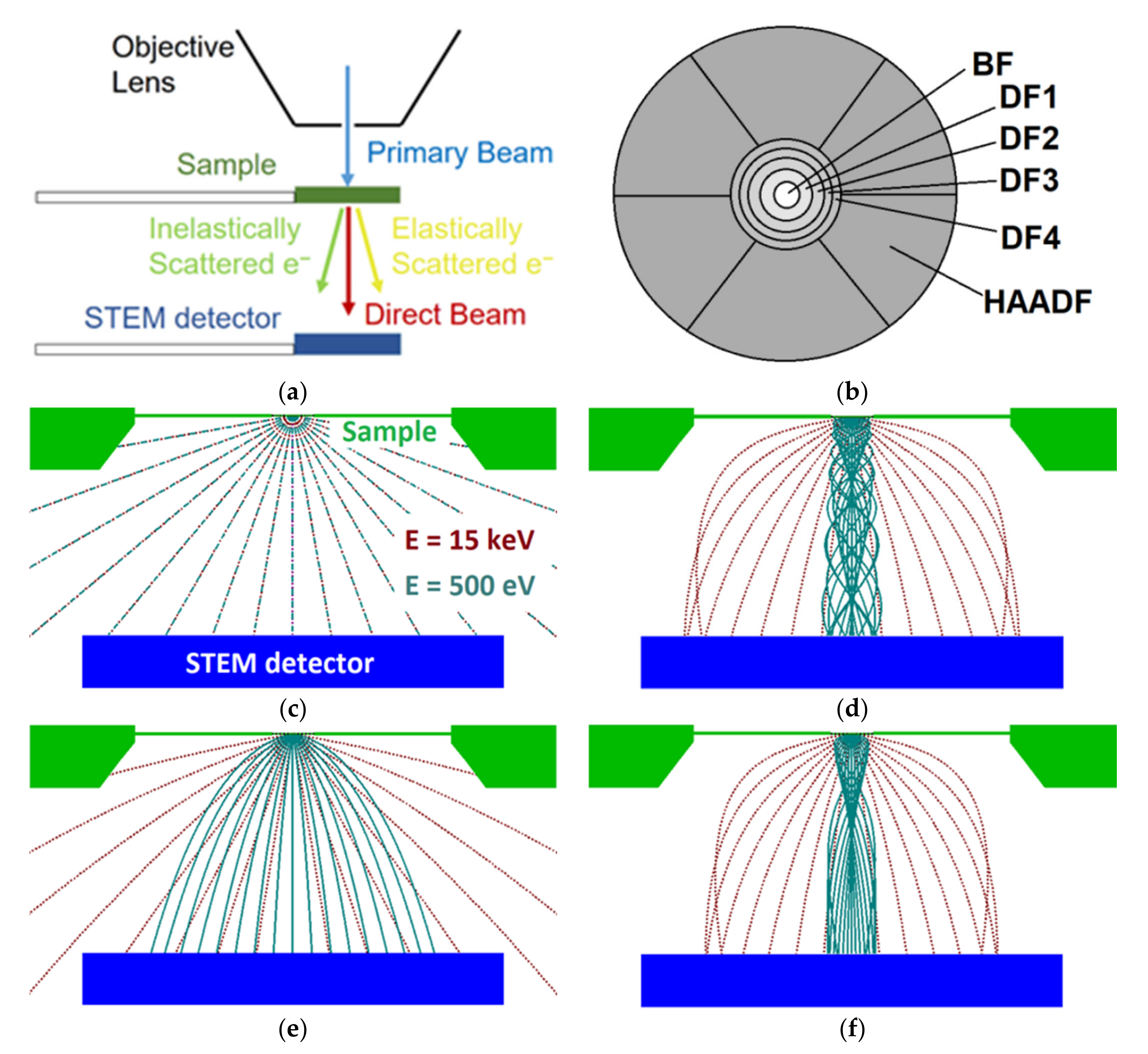
2.1. Microscope Imaging Modes
2.2. STEM Segmented Detector Measurement

2.3. 2D-PAD Measured Data and Their Processing
2.4. MC Simulations
2.5. Processing of MC Data
2.6. Samples
3. Results
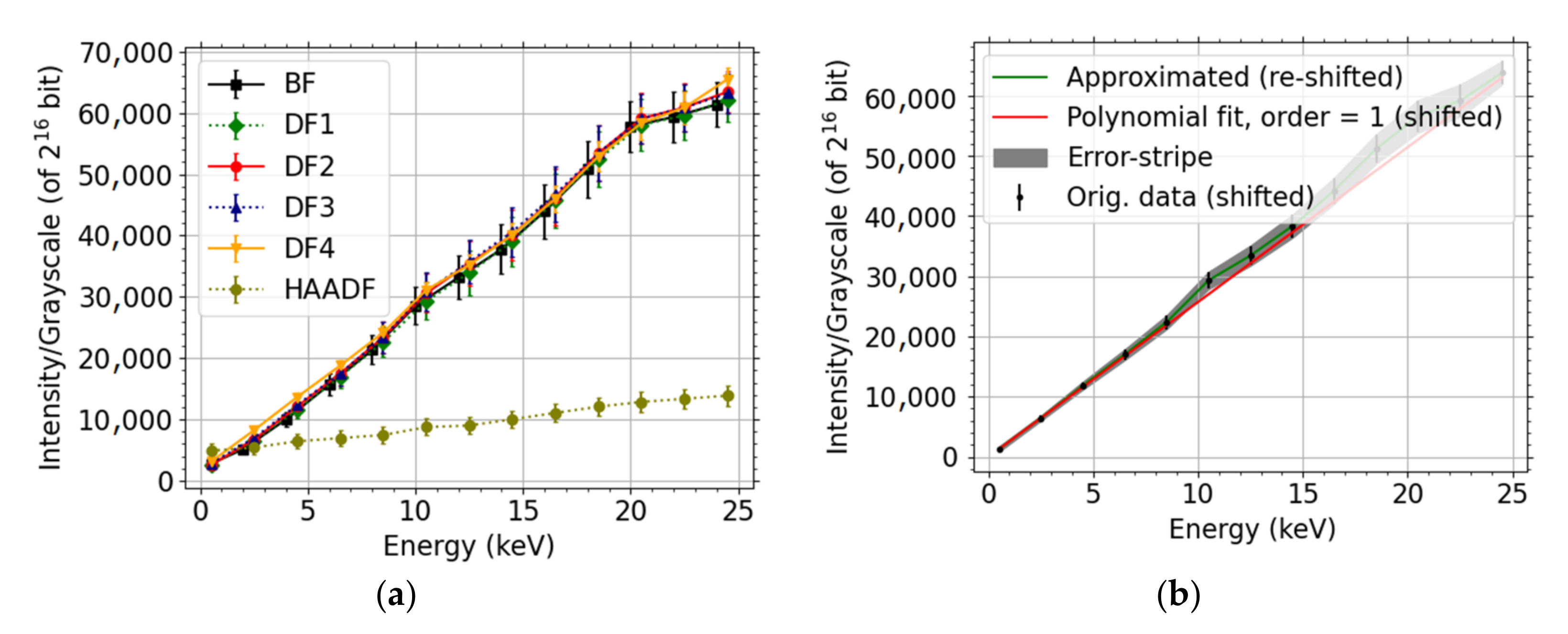
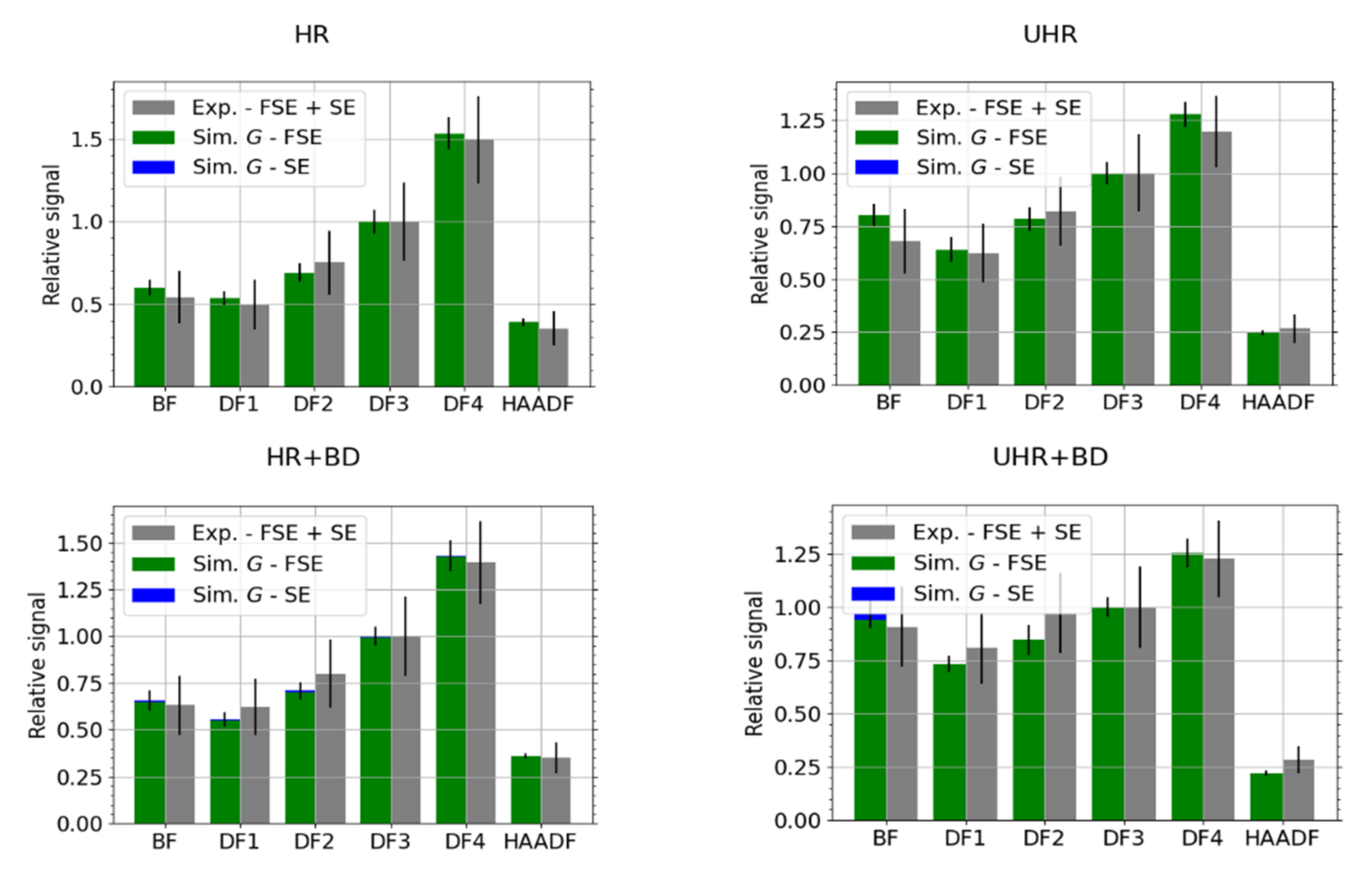
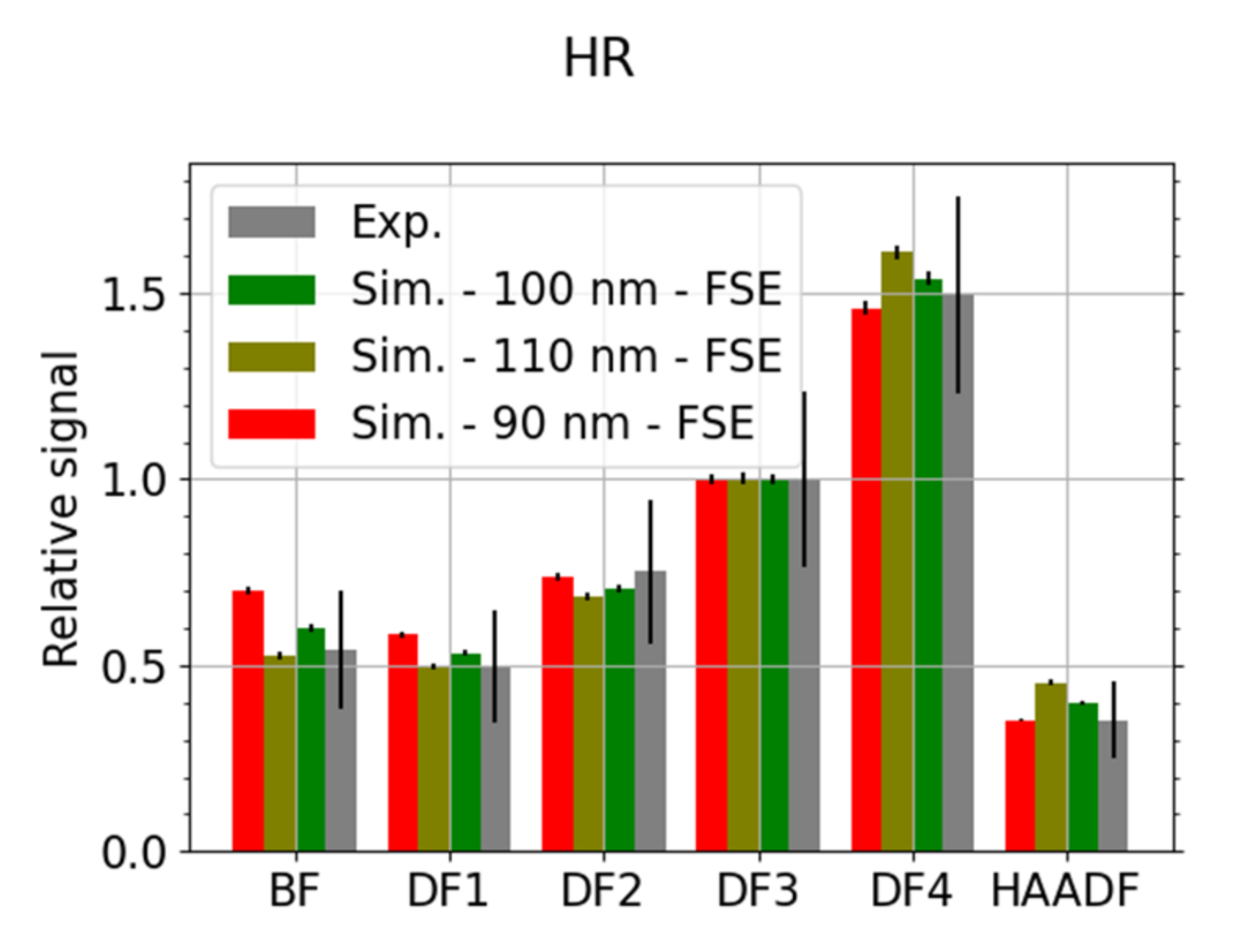
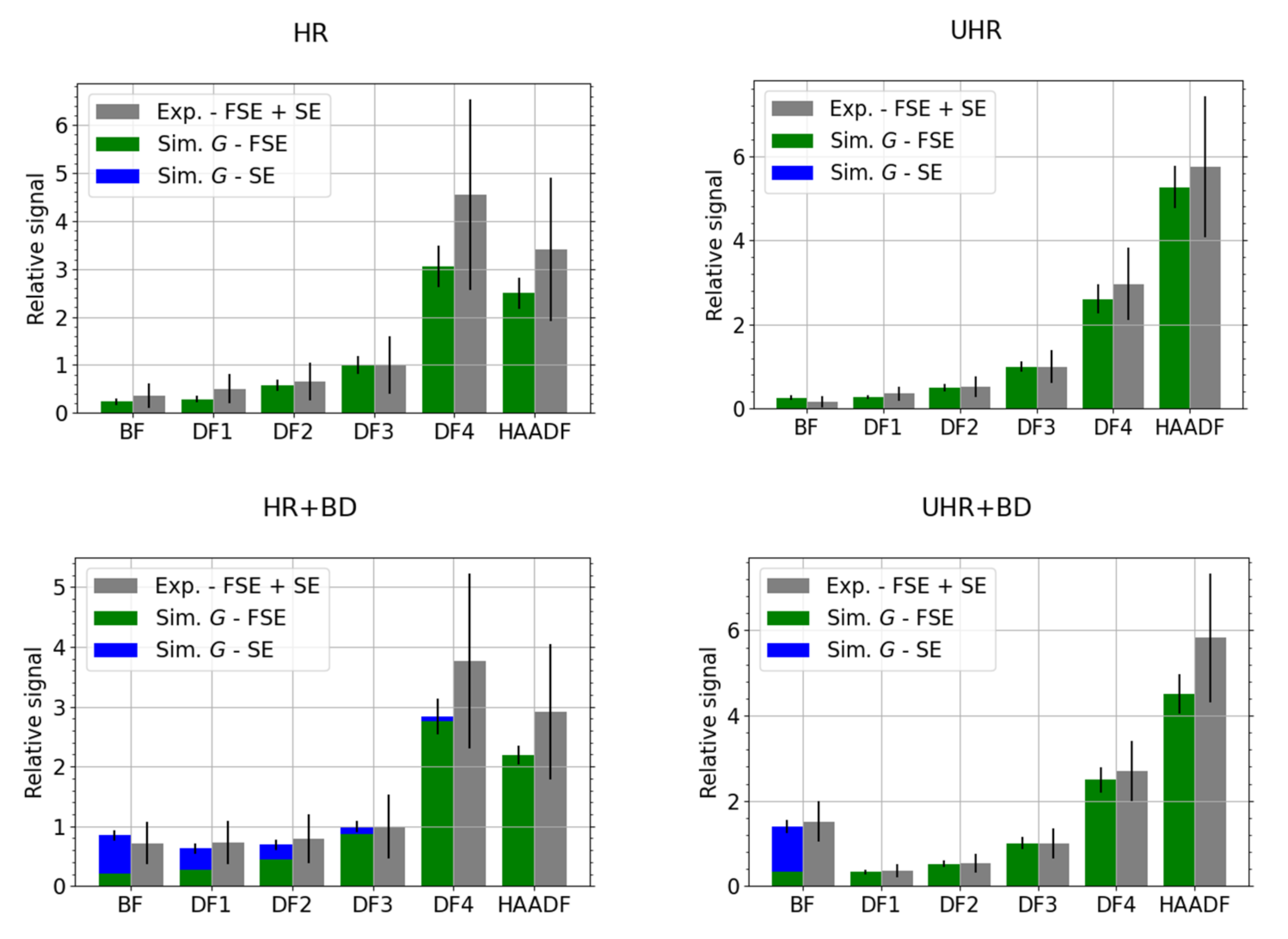
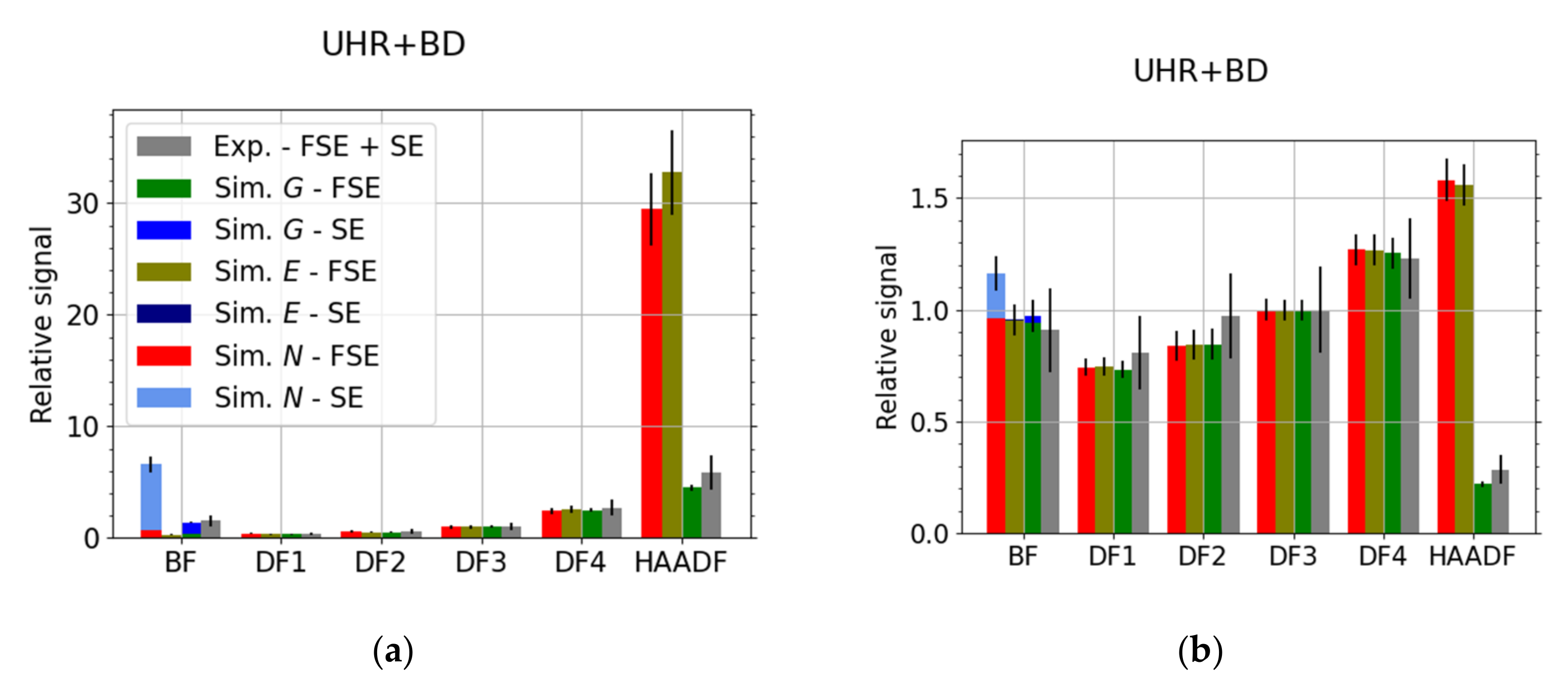
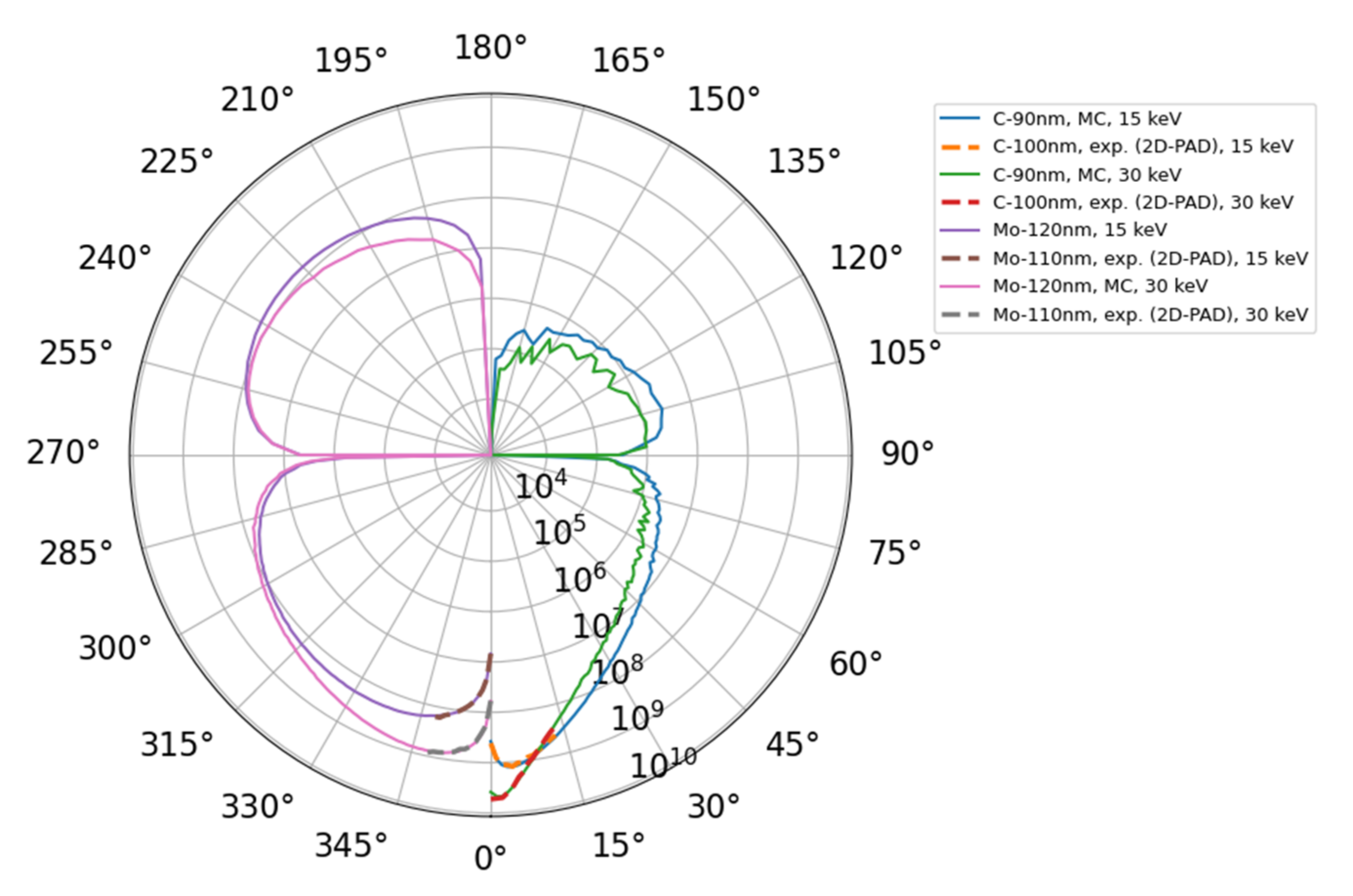
3.1. STEM Detector
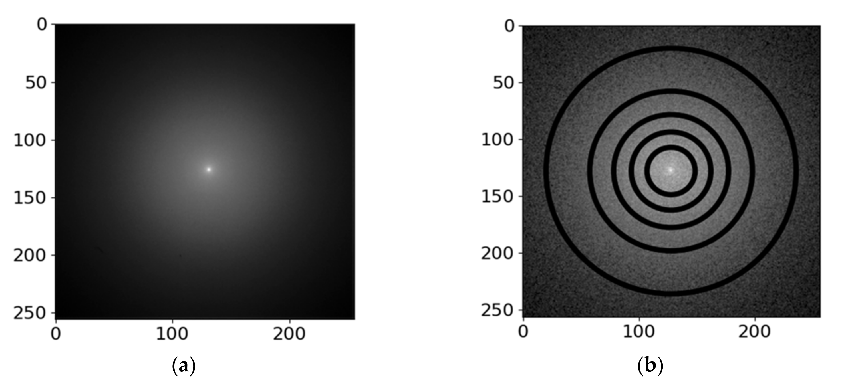
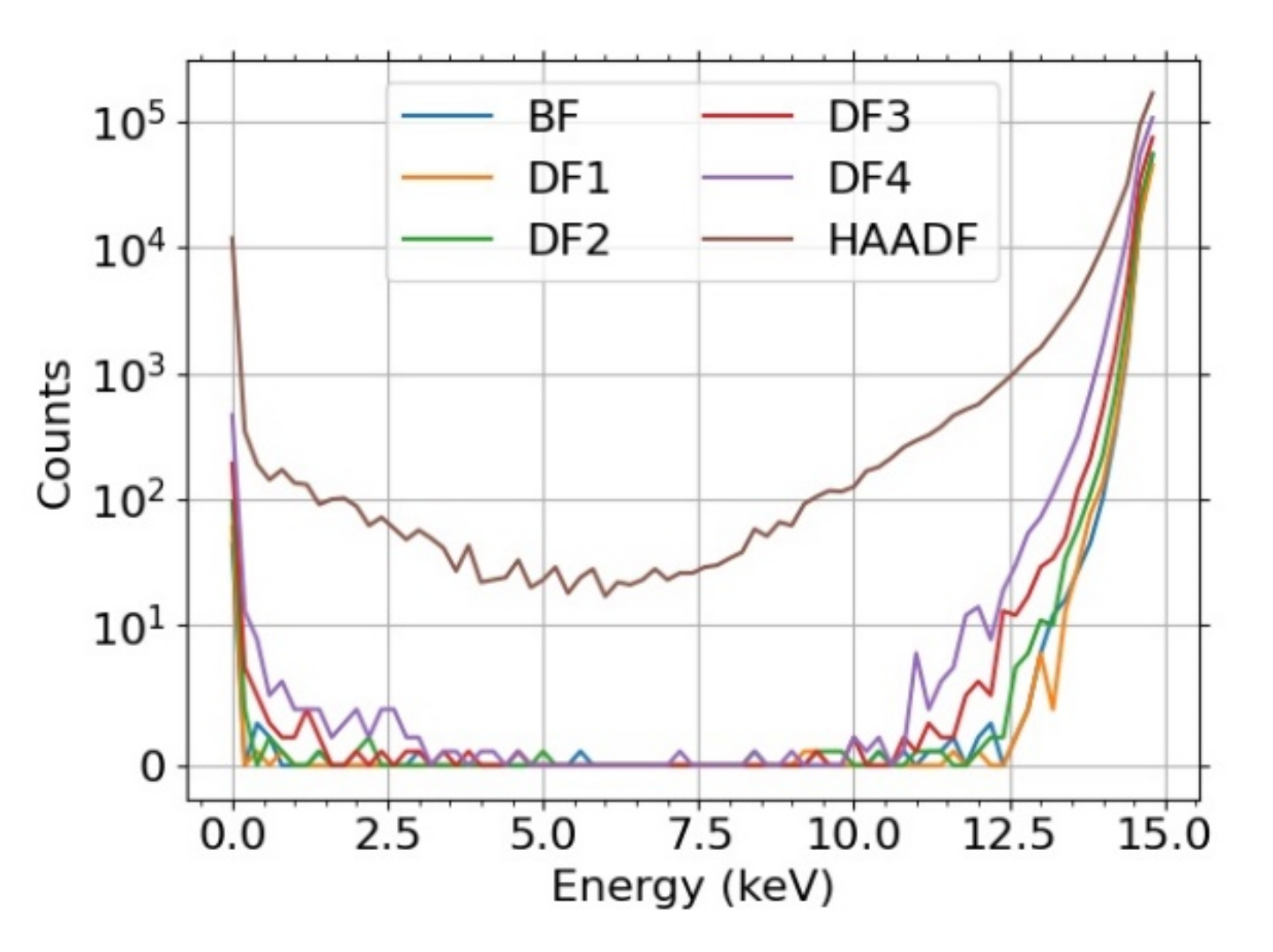
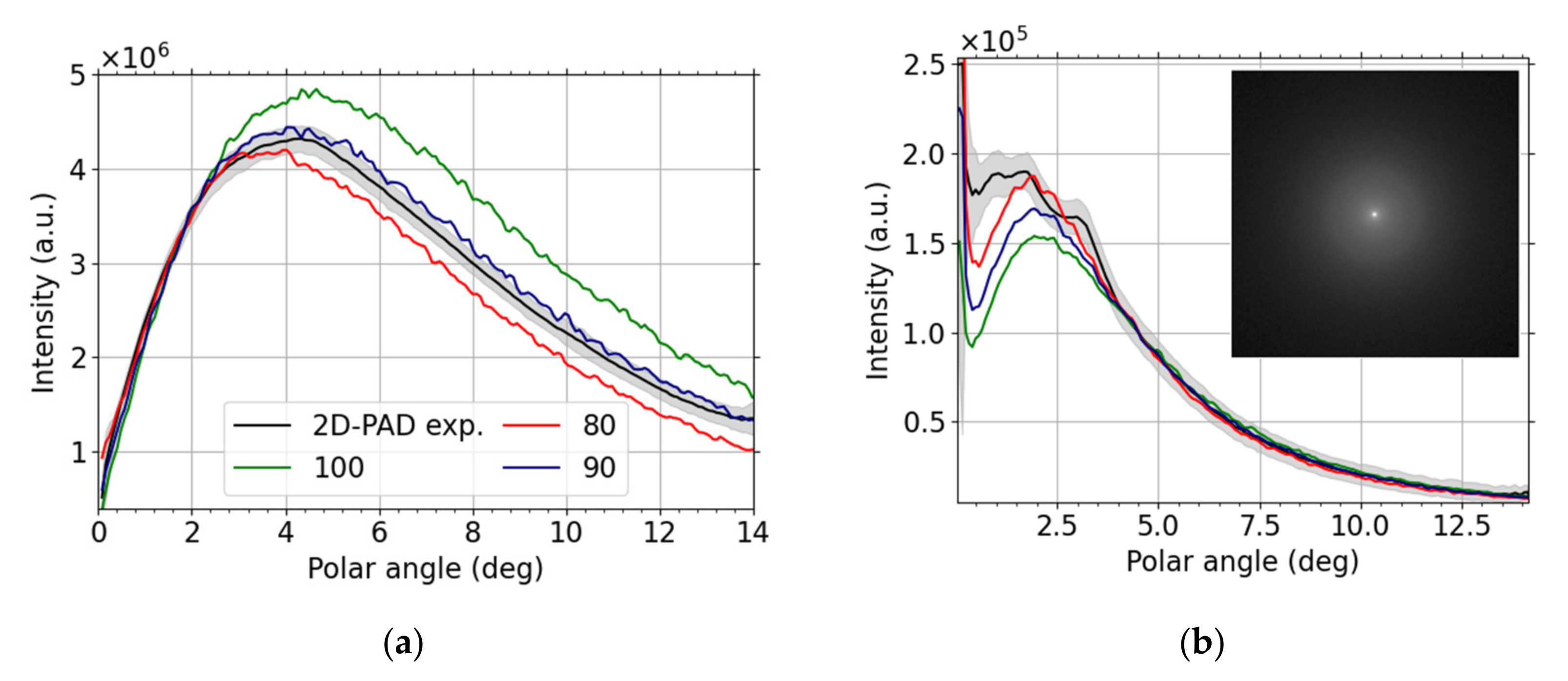
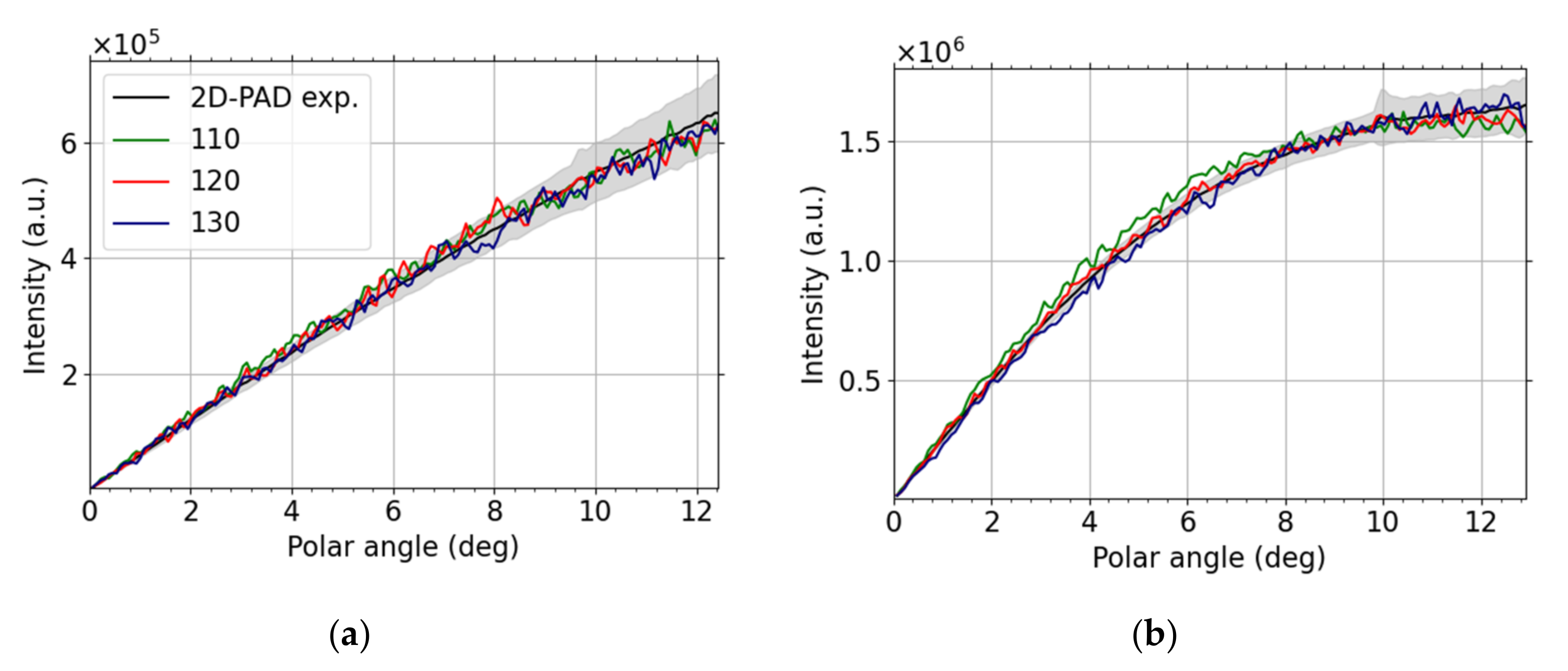
3.2. 2D-PAD Detector
4. Discussion
5. Conclusions
Author Contributions
Funding
Data Availability Statement
Acknowledgments
Conflicts of Interest
References
- MacArtur, K.E. The Use of Annular Dark-Field Scanning Transmission Electron Microscopy for Quantitative Characterisation. Johns. Matthey Technol. Rev. 2016, 60, 117–131. [Google Scholar] [CrossRef]
- Young, R.J.; Buxbaum, A.; Peterson, B.; Schampers, R. Application of In-situ Sample Preparation and Modeling of SEM-STEM Imaging. In Proceedings of the 34th International Symposium for Testing and Failure Analysis, Portland, OR, USA, 2–6 November 2008; pp. 320–327. [Google Scholar] [CrossRef]
- Crewe, A.V.; Wall, J.; Langmore, J. Visibility of single atoms. Science 1970, 168, 1338–1340. [Google Scholar] [CrossRef]
- Krivanek, O.; Chisholm, M.F.; Nicolosi, V.; Pennycook, T.J.; Corbin, G.J.; Dellby, N.; Murfitt, M.F.; Own, C.S.; Szilagyi, Z.S.; Oxley, M.P.; et al. Atom-by-atom structural and chemical analysis by annular dark-field electron microscopy. Nature 2010, 464, 571–574. [Google Scholar] [CrossRef] [Green Version]
- Yamashita, S.; Kikkawa, J.; Yanagisawa, K.; Nagai, T.; Ishizuka, K.; Kimoto, K. Atomic number dependence of Z contrast in scanning transmission electron microscopy. Sci. Rep. 2018, 8, 12325. [Google Scholar] [CrossRef]
- Müllerová, I.; Frank, L. Scanning low energy electron microscopy. In Advances in Imaging and Electron Physics; Hawkes, P.W., Ed.; Elsevier: San Diego, CA, USA, 2003; Volume 128, pp. 309–443. [Google Scholar]
- Frank, L.; Hovorka, M.; Mikmeková, Š.; Mikmeková, E.; Mullerová, I.; Pokorná, Z. Scanning Electron Microscopy with Samples in an Electric Field. Materials 2012, 5, 2731–2756. [Google Scholar] [CrossRef] [Green Version]
- Frank, L.; Hovorka, M.; Konvalina, I.; Mikmeková, Š.; Müllerová, I. Very low energy scanning electron microscopy. Nucl. Instrum. Methods Phys. Res. A 2011, 645, 46–54. [Google Scholar] [CrossRef]
- Konvalina, I.; Müllerová, I. Properties of the cathode lens combined with a focusing magnetic/immersion-magnetic lens. Nucl. Instrum. Methods Phys. Res. Sect. A 2011, 645, 55–59. [Google Scholar] [CrossRef]
- Müllerová, I.; Konvalina, I. Collection of secondary electrons in scanning electron microscopes. J. Microsc. 2009, 236, 203–210. [Google Scholar] [CrossRef] [PubMed]
- Müllerová, I.; Hovorka, M.; Konvalina, I.; Unconvsky, M.; Frank, L. Scanning transmission low-energy electron microscopy. IBM J. Res. Dev. 2011, 55, 2:1–2:6. [Google Scholar] [CrossRef]
- Fialová, D.; Skoupý, R.; Drozdová, E.; Paták, A.; Piňos, J.; Šín, L.; Beňuš, R.; Klíma, B. The Application of Scanning Electron Microscopy with Energy-Dispersive X-Ray Spectroscopy (SEM-EDX) in Ancient Dental Calculus for the Reconstruction of Human Habits. Microsc. Microanal. 2017, 23, 1207–1213. [Google Scholar] [CrossRef] [Green Version]
- Materna Mikmeková, E.; Müllerová, I.; Frank, L.; Paták, A.; Polčák, J.; Sluyterman, S.; Lejeune, M.; Konvalina, I. Low-energy electron microscopy of graphene outside UHV: Electron-induced removal of PMMA residues used for graphene transfer. J. Electron. Spectrosc. Relat. Phenom. 2020, 241, 146873. [Google Scholar] [CrossRef]
- Müllerová, I.; Hovorka, M.; Frank, L. A method of imaging ultrathin foils with very low energy electrons. Ultramicroscopy 2012, 119, 78–81. [Google Scholar] [CrossRef] [PubMed]
- MacLaren, I.; Macgregor, T.; Allen, C.S.; Kirkland, A.I. Detectors—The ongoing revolution in scanning transmission electron microscopy and why this important to material characterization. APL Mater. 2020, 8, 110901. [Google Scholar] [CrossRef]
- Ooe, K.; Seki, T.; Ikuhara, Y.; Shibata, N. High contrast STEM imaging for light elements by an annular segmented detector. Ultramicroscopy 2021, 220, 113133. [Google Scholar] [CrossRef] [PubMed]
- Skoupý, R.; Fořt, T.; Krzyzanek, V. Nanoscale Estimation of Coating Thickness on Substrates via Standardless BSE Detector Calibration. Nanomaterials 2020, 10, 332. [Google Scholar] [CrossRef] [PubMed] [Green Version]
- Sun, C.; Müller, E.; Meffert, M.; Gerthsen, D. On the Progress of Scanning Transmission Electron Microscopy (STEM) Imaging in a Scanning Electron Microscope. Microsc. Microanal. 2018, 24, 1–8. [Google Scholar] [CrossRef]
- Kundrat, V.; Patak, A.; Pinkas, J. Preparation of ultrafine fibrous uranium dioxide by electrospinning. J. Nucl. Mater. 2020, 528, 151877. [Google Scholar] [CrossRef]
- Frank, L.; Nebesářová, J.; Vancová, M.; Paták, A.; Müllerová, I. Imaging of tissue sections with very slow electrons. Ultramicroscopy 2015, 148, 146–150. [Google Scholar] [CrossRef]
- Merli, P.G.; Morandi, V. Low-Energy STEM of Multilayers and Dopand Profiles. Microsc. Microanal. 2005, 11, 97–104. [Google Scholar] [CrossRef] [Green Version]
- Vystavěl, T.; Stejskal, P.; Unčovský, M.; Stephens, C. Tilt-free EBSD. Microsc. Microanal. 2018, 24, 1126–1127. [Google Scholar] [CrossRef] [Green Version]
- Holzer, J.; Marshall, A.; Stejskal, P.; Stephens, C.; Vystavěl, T. Large area EBSD mapping using a tilt-free configuration and direct electron detection sensor. Microsc. Microanal. 2021, 27, 1832–1835. [Google Scholar] [CrossRef]
- Caplins, B.W.; Holm, J.D.; Keller, R.R. Transmission imaging with a programmable detector in a scanning electron microscope. Ultramicroscopy 2019, 196, 40–48. [Google Scholar] [CrossRef]
- Krivanek, O.L.; Dellby, N.; Murffitt, M.F. Aberration correction in electron microscopy. In Handbook of Charged Particle Optics, 2nd ed.; Orloff, J., Ed.; CRC Press: Boca Raton, FL, USA, 2008. [Google Scholar]
- Humphry, M.J.; Kraus, B.; Hurst, A.C.; Maiden, A.M.; Rodenburg, J.M. Ptychographic electron microscopy using high-angle dark-field scattering for sub-nanometre resolution imaging. Nat. Commun. 2012, 3, 730. [Google Scholar] [CrossRef] [Green Version]
- Hammersley, J.M.; Handscomb, D.C. Monte Carlo methods. In Methuen’s Monographs on Applied Probability and Statistics; Bartlett, M.S., Ed.; Methuen & Co Ltd.: London, UK, 1975. [Google Scholar]
- Bielajew, A.F. Fundamentals of the Monte Carlo method for Neutral and Charged Particle Transport; The University of Michigan: Ann Arbor, MI, USA, 2001. [Google Scholar]
- Ridky, J. Can we observe the quark gluon plasma in cosmic ray showers. Astropart. Phys. 2004, 17, 355–365. [Google Scholar] [CrossRef] [Green Version]
- Kyrakou, I.; Incerti, S.; Francis, Z. Technical Note: Improvements in geant4 energy-loss model and the effect on low-energy electron transport in liquid water. Med. Phys. 2015, 42, 3870–3876. [Google Scholar] [CrossRef]
- Reimer, L. Scanning Electron Microscopy. Physics of Image Formation and Microanalysis; Springer series in Optical Sciences; Reimer, L., Ed.; Springer: Berlin/Heidelberg, Germany, 1998. [Google Scholar] [CrossRef]
- Stary, V. Monte-Carlo Simulation in Electron Microscopy and Spectroscopy. In Applications of Monte Carlo Method in Science and Engineering; InTech: Shanghai, China, 2011. [Google Scholar] [CrossRef] [Green Version]
- Salvat, F.; Llovet, X. Monte Carlo simulation and fundamental quantities. IOP Conf. Ser. Mater. Sci. Eng. 2018, 304, 012014. [Google Scholar] [CrossRef] [Green Version]
- Skoupý, R. Quantitative Imaging in Scanning Electron Microscope. Ph.D. Thesis, Brno University of Technology, Brno, Czech Republic, 2020; 100p. [Google Scholar]
- Agostinelli, S.; Allison, J.; Amako, K.; Apostolakis, J.; Araujo, H.; Arce, P.; Asai, M.; Axen, D.; Banerjee, S.; Barrand, G.; et al. Geant4—A simulation toolkit. Nucl. Instrum. Methods Phys. Res. A Accel. Spectrom. Detect. Assoc. Equip. 2003, 506, 250–303. [Google Scholar] [CrossRef] [Green Version]
- Kieft, E.; Bosch, E. Refinement of Monte Carlo simulations of electron–specimen interaction in low-voltage SEM. J. Phys. D Appl. Phys. 2008, 41, 215310. [Google Scholar] [CrossRef]
- Dwyer, C. Quantitative annular dark-field imaging in the scanning transmission electron microscope—A review. J. Phys. Mater. 2021, 4, 042006. [Google Scholar] [CrossRef]
- Walker, C.; Konvalina, I.; Mika, F.; Frank, L.; Müllerová, I. Quantitative comparison of simulated and measured signals in the STEM mode of a SEM. Nucl. Instrum. Methods Phys. Res. B 2018, 415, 17–24. [Google Scholar] [CrossRef]
- MacArtur, K.E.; Jones, L.B.; Nellist, P.D. How flat is your detector? Non-uniform annular detector sensitivity in STEM quantification. J. Phys. Conf. Ser. 2014, 522, 012018. [Google Scholar] [CrossRef] [Green Version]
- He, D.S.; Li, Z.Y. A practical approach to quantify the ADF detector in STEM. J. Phys. Conf. Ser. 2014, 522, 012017. [Google Scholar] [CrossRef] [Green Version]
- Krause, F.F.; Schowalter, M.; Grieb, T.; Müller-Caspary, K.; Mehrtens, T.; Rosenauer, A. Effects of instrument imperfections on quantitative scanning transmission electron microscopy. Ultramicroscopy 2016, 161, 146–160. [Google Scholar] [CrossRef] [PubMed]
- Mika, F.; Walker, C.G.H.; Konvalina, I.; Müllerová, I. Imaging with STEM Detector, Experiments vs. Simulation. Microsc. Microanal. 2015, 21, 66–71. [Google Scholar] [CrossRef] [Green Version]
- Thermo Fisher Scientific. Available online: https://corporate.thermofisher.com/us/en/index.html (accessed on 6 December 2021).
- Konvalina, I.; Mika, F.; Krátký, S.; Materna Mikmeková, E.; Müllerová, I. In-Lens Band-Pass Filter for Secondary Electrons in Ultrahigh Resolution SEM. Materials 2019, 12, 2307. [Google Scholar] [CrossRef] [PubMed] [Green Version]
- Salvat, F.; Fernández-Varea, J.M.; Sempau, J. PENELOPE-2006: A Code System for Monte Carlo Simulation of Electron and Photon Transport; Nuclear Energy Agency, Organization for Economic Co-operation and Development: Barcelona, Spain, 2006; ISBN 92-64-02301-1. [Google Scholar]
- Cullen, D.E.; Hubbell, J.H.; Kissel, L. EPDL97: The Evaluated Photon Data Library, ′97 Version; UCRL-50400; University of California, Lawrence Livermore National Laboratory: Livermore, CA, USA, 1997; Volume 6. [Google Scholar]
- Zlámal, J.; Lencová, B. Development of the program EOD for design in electron and ion microscopy. Nucl. Instrum. Methods A 2011, 645, 278–282. [Google Scholar] [CrossRef]
- Martinez, G.T.; Jones, L.; De Backer, A.; Béché, A.; Verbeeck, J.; Van Aert, S.; Nellist, P.D. Quantitative STEM normalisation: The importance of the electron flux. Ultramicroscopy 2015, 159, 46–58. [Google Scholar] [CrossRef]
- Virtanen, P.; Gommers, R.; Oliphant, T.E.; Haberland, M.; Reddy, T.; Cournapeau, D.; Burovski, E.; Peterson, P.; Weckesser, W.; Bright, J.; et al. SciPy 1.0: Fundamental algorithms for scientific computing in Python. Nat. Methods 2020, 17, 261. [Google Scholar] [CrossRef] [Green Version]
- Harris, C.R.; Millman, K.J.; van der Walt, S.J.; Gommers, R.; Virtanen, P.; Cournapeau, D.; Wieser, E.; Taylor, J.; Berg, S.; Smith, N.J.; et al. Array programming with NumPy. Nature 2020, 585, 357–362. [Google Scholar] [CrossRef]
- Hunter, J.D. Matplotlib: A 2D Graphics Environment. Comput. Sci. Eng. 2007, 9, 90–95. [Google Scholar] [CrossRef]
- Lebow Company, Thin Films. Available online: https://lebowcompany.com/thin-films (accessed on 6 December 2021).
- Fallon, P.J.; Veerasamy, V.S.; Davis, C.A.; Robertson, J.; Amaratunga, G.A.J.; Milne, W.I.; Koskinen, J. Properties of filtered-ion-beam-deposited diamondlike carbon as a function of ion energy. Phys. Rev. B 1994, 49, 2287. [Google Scholar] [CrossRef]
- Bhattarai, B.; Pandey, A.; Drabold, D.A. Evolution of amorphous carbon across densities: An inferential study. Carbon 2018, 131, 168–174. [Google Scholar] [CrossRef] [Green Version]
- Beyer, A.; Straubinger, R.; Belz, J.; Volz, K. Local sample thickness determination via scanning transmission electron microscopy defocus series. J. Microsc. 2016, 262, 171–177. [Google Scholar] [CrossRef]
- Liu, J.; Lozano-Perez, S.; Wilkinson, A.J.; Grovenor, C.R.M. On the depth resolution of transmission Kikuchi diffraction (TKD) analysis. Ultramicroscopy 2019, 205, 5–12. [Google Scholar] [CrossRef] [Green Version]
- Konvalina, I.; Daniel, B.; Zouhar, M.; Paták, A.; Müllerová, I.; Frank, L.; Piňos, J.; Průcha, L.; Radlička, T.; Werner, W.S.M.; et al. Low-Energy Electron Inelastic Mean Free Path of Graphene Measured by a Time-of-Flight Spectrometer. Nanomaterials 2021, 11, 2435. [Google Scholar] [CrossRef] [PubMed]
- Vystavel, T.; Stejskal, P.; Uncovsky, M. Measurement and Andpointing of Sample Thickness. U.S. Patent US 10.978.272B2, 13 April 2021. [Google Scholar]
- Zhang, H.; Egerton, R.F.; Malac, M. Local Thickness Measurement in TEM. Microsc. Microanal. 2010, 16, 344–345. [Google Scholar] [CrossRef] [Green Version]
- Morandi, V.; Merli, P.G. Contrast and resolution versus specimen thickness in low energy scanning transmission electron microscopy. J. Appl. Phys. 2007, 101, 114917. [Google Scholar] [CrossRef]
- Volkenandt, T.; Müller, E.; Gerthsen, D. Sample Thickness Determination by Scanning Transmission Electron Microscopy at Low Electron Energies. Microsc. Microanal. 2014, 20, 142–143. [Google Scholar] [CrossRef] [Green Version]


| “Order”\Source | C 100 nm, 2D-PAD | Graphene | Bragg Formula (hkl) |
|---|---|---|---|
| “1st” | 1.0 | - | 1.0 (100) |
| “2nd” | 1.7 | 1.8 | 1.7 (110) |
| “3rd” | 3.0 | 3.1 | 2.9 (300) |
Publisher’s Note: MDPI stays neutral with regard to jurisdictional claims in published maps and institutional affiliations. |
© 2021 by the authors. Licensee MDPI, Basel, Switzerland. This article is an open access article distributed under the terms and conditions of the Creative Commons Attribution (CC BY) license (https://creativecommons.org/licenses/by/4.0/).
Share and Cite
Konvalina, I.; Paták, A.; Zouhar, M.; Müllerová, I.; Fořt, T.; Unčovský, M.; Materna Mikmeková, E. Quantification of STEM Images in High Resolution SEM for Segmented and Pixelated Detectors. Nanomaterials 2022, 12, 71. https://doi.org/10.3390/nano12010071
Konvalina I, Paták A, Zouhar M, Müllerová I, Fořt T, Unčovský M, Materna Mikmeková E. Quantification of STEM Images in High Resolution SEM for Segmented and Pixelated Detectors. Nanomaterials. 2022; 12(1):71. https://doi.org/10.3390/nano12010071
Chicago/Turabian StyleKonvalina, Ivo, Aleš Paták, Martin Zouhar, Ilona Müllerová, Tomáš Fořt, Marek Unčovský, and Eliška Materna Mikmeková. 2022. "Quantification of STEM Images in High Resolution SEM for Segmented and Pixelated Detectors" Nanomaterials 12, no. 1: 71. https://doi.org/10.3390/nano12010071