
Abstract
This review delves into the intricacies of the interfaces formed between two-dimensional (2D) materials and metals, exploring a realm rich with fundamental insights and promising applications. Historically, our understanding of 2D materials emanated from studies employing dielectric substrates or suspended samples. However, integrating metals in the exfoliation and growth processes of 2D materials has opened up new avenues, unveiling various shades of interactions ranging from dispersive forces to covalent bonding. The resulting modifications in 2D materials, particularly transition metal dichalcogenides (TMDCs), offer more than a theoretical intrigue. They bear substantial implications for (opto)electronics, altering Schottky barrier heights and contact resistances in devices. We explore metal-mediated methods for TMDC exfoliation, elucidating the mechanisms and their impact on TMDC-metal interactions. Delving deeper, we scrutinize the fundamentals of these interactions, focusing primarily on MoS2 and Au. Despite the recent surge of interest and extensive studies, critical gaps remain in our understanding of these intricate interfaces. We discuss controversies, such as the changes in Raman or photoemission signatures of MoS2 on Au, and propose potential explanations. The interplay between charge redistribution, substrate-induced bond length variations, and interface charge transfer processes are examined. Finally, we address the intriguing prospect of TMDC phase transitions induced by strongly interacting substrates and their implications for contact design.
Export citation and abstract BibTeX RIS

Original content from this work may be used under the terms of the Creative Commons Attribution 4.0 license. Any further distribution of this work must maintain attribution to the author(s) and the title of the work, journal citation and DOI.
1. Introduction
The isolation of individual atomically thin monolayers from their bulk layered crystals opened up new avenues in nanoscience and nanotechnology [1, 2]. The sudden accessibility of two-dimensional (2D) materials enabled their spread to laboratories worldwide and even to the first commercial products [3]. One of the main drawbacks, and, at the same time, one of the most important features, of 2D materials is the extreme sensitivity to their environment. This includes the atmosphere they are in, the substrate on which they lie, and particles, molecules, or other layers surrounding them. The environment can easily modify the crystal structure and (opto)electronic properties of 2D materials globally and locally through lattice deformation and charge or energy transfer. Such immense responsiveness to external stimuli stems from the mostly surface nature of the 2D materials that causes, for example, their low bending rigidity [4] or low charge carrier density [5].
The issues with the underlying substrate accompany 2D materials, namely graphene, since its first isolation. While the initial preparation of graphene took place on the standard substrate used in the semiconductor industry, i.e. SiO2/Si [5], the most promising method of scalable preparation of high-quality graphene by chemical vapor deposition (CVD) uses a metal catalyst (most commonly Cu) as the substrate [6]. The need for subsequent transfer of the as-grown graphene to a dielectric substrate generates additional costs in the production, and, importantly, damages and contaminates the transferred graphene [7]. Even the differences between various dielectric substrates determine the resulting properties of the graphene resting on top of them. Carrier mobility in graphene is the classical example, with values ranging from  cm2 V−1 s−1 on SiO2/Si [8] to
  cm2 V−1 s−1 on hexagonal boron nitride (hBN) [9]. The difference is caused by heterogeneities stemming from (i) localized pools of charge carriers at the interface, creating the so-called 'charge puddles' [10], (ii) local variations in graphene lattice deformation due to uneven adhesion to the substrate [11], or (iii) differences in the level of charge screening in environments with substantially varied dielectric constant [12].
The environment-related changes in other 2D materials, e.g. transition metal dichalcogenides (TMDC), are no less dramatic [13]. The substrate affects the doping level (similarly to graphene) and the decay rates of the excitonic transition in TMDCs such as MoS2 and WSe2 [14–16], regulates charge transfer processes between TMDC and molecular dopants [17], or acts as a mirror for excitons [18]. In addition, the frequency-dependent dielectric function of the surrounding media influences the dynamic screening of excitons in TMDCs, as shown for WS2 [19].
Note that not only the substrate below the 2D material but also the airborne contamination adsorbed on top of it and trapped between it and the substrate affects the 2D material's properties. Contamination is always present at the interface [20] and at any exposed surface [21] of samples prepared outside ultra-high vacuum (UHV). Even though its presence is usually detrimental, e.g. to transport properties as in the case of graphene mentioned above, bubbles filled by the contaminants find utilization as tunable photoluminescence (PL) emitters [22].
The way to exert control over the environmental effects is to envelop the 2D layer by strongly interacting surfaces of other materials. These can be other 2D materials, thereby forming a purely 2D van der Waals (vdW) heterostructure [23], or 3D (bulk) materials with defined crystalline faces to create a mixed-dimensional vdW assembly [24]. The possible properties modification of such heterostructures are endless. They depend both on the composition of the layers and their stacking order, i.e. how their lattices are aligned to each other. Some of the seminal examples include the superconductivity in bilayer graphene where the two layers are rotated by a 'magic angle' ( ) [25] or ferroelectricity in marginally twisted TMDCs homobilayers [26].
Several techniques are employed for the preparation and/or controlled placement of 2D monolayers: direct exfoliation on SiO2 substrates and polydimethylsiloxane stamps, liquid-phase exfoliation, CVD, pulsed laser deposition (PLD), molecular beam epitaxy (MBE), etc [27, 28]. Usually, the highest-quality 2D monolayers are obtained by direct exfoliation from bulk crystals on flat dielectric substrates, but the flakes commonly reach only tens of micrometers in lateral size. Larger monolayers can be obtained using alternative techniques, but the optoelectronic and chemical properties of the thus-prepared materials are altered due to the introduction of strain, bubbles, wrinkles, and defects [3].
Recently, a novel metal-mediated exfoliation technique opened a new pathway to centimeter-sized monolayer crystals [29–31]. On the one hand, atomically flat monolayers, with low density of defects, wrinkles, or bubbles can be obtained. On the other hand, the interaction with the underlying (or overlying) metal gives rise to not yet fully comprehended physicochemical phenomena. Besides the puzzling fundamental aspects, this unexpected marriage has already been shown to yield promising results that could be exploited in the near future. For example, Au atoms at the MoS2-Au interface can substitute S vacancies to cause non-volatile memristive switching [32]. The strong MoS2-Au interaction also modifies the bonding of the top S atoms, thereby enhancing the reactivity towards diazonium molecules [33]. Finally, monolayer TMDCs on Au represent an intriguing system from the (photo)electrochemistry perspective [34].
In this review, we focus on the properties of 2D monolayers in contact with metal surfaces, with a special emphasis on the TMDC material family. A TMDC monolayer is made of three atomic layers with the general formula MX2, where M is the transition metal (such as Mo, W, Ta, Nb, etc) and X the chalcogen (S, Se, Te). In each MX2 monolayer, the central layer of metal atoms is covalently bonded to chalcogen atoms, which form the two adjacent layers (figure 1) [27]. There are only two atom coordination geometries in the monolayer, the trigonal prismatic (D point group), also referred to as the 1H phase, and the octahedral (D
 point group), referred to as the 1T phase (the 1Tʹ usually denotes the distorted octahedral geometry). For the bulk TMDC crystal, formed by vdW stacking of the monolayers, three main different polymorphs exist (1T, 2H, and 3R), reflecting the stacking sequence [35]. The range of elemental compositions and structural polytypes leads to a large portfolio of MX2 properties. The band structure character varies from metallic, semimetallic, to semiconducting, with either a direct or indirect band gap type for the latter [27]. On the one hand, metallic TMDCs offer many exciting possibilities following the discovery of correlated states like charge density waves (CDW), superconductivity, and many other topological phases [36]. These fundamental properties are usually studied at low temperatures by scanning tunneling microscopy and/or spectroscopy (STM/STS), angle-resolved photoelectron spectroscopy (ARPES), transport, or, occasionally, by Raman spectroscopy, e.g. for NbSe2 [37]. On the other hand, for (M = Mo, W, X = S, Se, Te) semiconducting TMDCs, their optoelectronic and excitonic properties have been the focus of research, for example, of the strong spin–orbit coupling that leads to valley-selective phenomena (valleytronics). In contrast to most of the low-temperature correlation physics in metallic TMDCs, the traits of the semiconducting TMDCs are accessible—to a certain degree—by room temperature/ambient pressure optical methods, such as Raman and PL spectroscopies, or, locally, by (photo)current atomic force microscopy (C-AFM), Kelvin probe force microscopy (KPFM), or tip-enhanced spectroscopies.

Figure 1. Schematic of the main scientific questions and characterization tools related to the investigation of 2D material-metal interaction addressed in this review.
Download figure:
Standard image High-resolution imageThe vast majority of knowledge about the fundamental properties of TMDCs has been gathered during studies that use dielectrics as substrates or on suspended samples. However, the metals that assist the large-area exfoliation or growth of TMDCs launched a new playground through orbital hybridization, energy transfer, strain, metal-induced gap states, and interfacial dipoles [38]. The interactions vary from long-range dispersive forces to covalent chemical bonding, depending on the TMDC, metal, and preparation of the interface. The changes imposed on the interacting TMDCs are not only interesting from the fundamental perspective, but their influence reaches applications, especially in engineering of (opto)electronic devices, due to the modulation of the Schottky barrier height and contact resistance [39]. We will first review the existing metal-mediated methods of TMDC exfoliation, the mechanism of the process, and its influence on the TMDC-metal interaction. The fundamentals of the interactions and the means of their investigation will be then scrutinized, emphasizing the most heated debates in the literature concerning primarily MoS2 and Au as a model system (figure 1). Finally, we will offer our opinions on selected challenges in this field.
2. Interface preparation
Monolayers of 2D materials on metallic substrates, particularly gold, have recently sparked a keen interest. Researchers developed different approaches to prepare these systems, including direct mechanical exfoliation, template stripping, metal-assisted exfoliation, and direct growth [40, 41]. 2D monolayers grown on metals in the latter case have been studied for over a decade. The growth methods range from the CVD [6, 7] to MBE, which has experienced large progress over the last years [42]. These methods enabled researchers to lay solid foundations for studying the 2D material/metal interface, particularly using surface-sensitive UHV-based methods (STM/STS/ARPES). Many of such findings are also valid for the interfaces prepared by mechanical exfoliation, as discussed below.
2.1. Exfoliation methods
Direct mechanical exfoliation relies on pressing an adhesive tape covered with bulk layered crystals onto a clean and flat metal surface (figure 2(a)). The first direct exfoliation of large-area TMDCs on Au [31] and metal-assisted exfoliation of MoS2 using Au [29] coincided with the theoretical prediction of strong binding and large interfacial strain between MoS2 and Au [43]. A follow-up on these pioneering studies showed that exfoliation of monolayers up to a centimeter in lateral size is achievable using high-quality parent bulk crystals, such as molybdenite [30]. Different gold deposition methods were successfully employed, including magnetron sputtering, electron beam evaporation, and thermal evaporation [44].
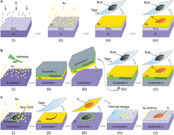
Figure 2. Schematic of the direct exfoliation, template-stripping exfoliation, and metal-assisted exfoliation. (a) Direct exfoliation starts with Ti adhesion layer deposition on a clean SiO2/Si wafer (i), followed by deposition of Au (ii). The tape with bulk layered crystals is then pressed onto the Au surface (iii) and removed to leave mostly monolayer material (iv). (b) Template-stripping exfoliation begins with the deposition of Au on a clean Si wafer (without the Ti) and gluing (i) another Si wafer on top of it (ii). The Si/adhesive/Au stack is mechanically separated from the bottom Si substrate (iii) and turned upside down, a tape with bulk layered crystals pressed onto it (iv), and removed to expose the monolayers (v). (c) Metal-assisted exfoliation relies on the deposition of Au directly onto a surface of the bulk layered crystal glued to a suitable substrate, typically Si (i). A thermal-release tape is pressed against the surface (ii) and peeled to remove the Au and a 2D monolayer adherent to it (iii). The tape is transferred to another target substrate, typically SiO2, and separated from Au by heat (iv). Finally, Au is chemically etched away to expose the monolayer (v).
Download figure:
Standard image High-resolution imageGood quality, continuous monolayers (1L) with lateral sizes of tens or hundreds of microns, are routinely prepared by direct exfoliation on Au with little optimization (figures 3(a)–(c)). The universal applicability of this method has been demonstrated for a wide range of different 2D materials, including chalcogenides, halides, thiophosphates, and single elements (such as phosphorene) [45, 46]. Interestingly, direct exfoliation does not work better, in comparison to exfoliation on oxygen plasma-cleaned SiO2, for the two most commonly studied 2D materials, graphene and hBN, with notable exceptions discussed below [47, 48]. This could be explained by the 4× (2×) smaller predicted binding energy of Au with graphene (hBN) as compared to MoS2 [49].

Figure 3. Optical images of large-area monolayers of 2D materials on metals. (a) MoS2 on Au prepared in air (authors' results). (b)–(c) RuCl3 and PtSe2 on Au prepared in air (adapted from [46]. CC BY 4.0). (d) MoS2 on Ag prepared in a glovebox (authors' results). (e) WSe2 on Ag prepared under UHV (adapted from [56]. CC BY 4.0). (f) Phosphorene, i.e. 1L of black phosphorus (BP) on Ag, prepared in a glovebox (adapted from [52]. CC BY 4.0). Samples in (a)–(f) were prepared by direct exfoliation. (g)–(i) MoS2 on Pd, Cu, and Ni, respectively, prepared by metal-assisted exfoliation ([57] John Wiley & Sons. © 2022 Wiley-VCH GmbH).
Download figure:
Standard image High-resolution imageTemplate stripping of Au deposited on a smooth surface [50], such as Si or SiO2, and a sacrificial wafer or glass slide are employed to provide fresh metal surfaces for 2D material exfoliation (figure 2(b)) [51–53]. A thermal release tape has also been used to pick the Au layer up from the Si substrate, press it onto the surface of a bulk layered material, and lift it off again with an exfoliated TMDC monolayer [54]. Li et al utilized the strong interaction of TMDCs with a gold mesh embedded in a polymer stamp to exfoliate the monolayers, weakly adhering to a polymer in between the Au pattern, directly on a weakly interacting substrate [55]. Due to the practical ease and relatively good crystal quality, direct mechanical exfoliation and template stripping of 2D materials using gold have become the most rapidly adopted methods to prepare large-area TMDC monolayers.
Metal-assisted exfoliation (figure 2(c)), used in one of the early reports [29] and dubbed a 'flip-chip' method by others later [58, 59], is another alternative. In this case, monolayer exfoliation is facilitated by the deposition of metals on top of bulk layered crystals, followed by peeling off the Au layer with a 2D monolayer attached. In another modification, the Au was deposited on top of CVD-grown WSe2 monolayer followed by its stripping to expose the 'buried' WSe2-Au interface [60]. The disadvantage of the flip-chip approach is the damage to the 2D materials incurred by the plasma, electron beam, and depositing atoms [61]. This is especially relevant to metal-semiconductor junctions, which exhibit strong Fermi level pinning in the case of metals deposited on MoS2, as opposed to tunable Schottky barriers in transferred contacts [62].
2.2. Exfoliation mechanism
Let us elaborate on the mechanism of the exfoliation process. Several strategies, such as oxygen plasma or heat treatment of the substrate, to increase the adhesion, are routinely used to enhance both the monolayer and bulk exfoliation yields on arbitrary substrates [28]. TMDCs bind stronger to Au than the individual layers do to each other in the bulk layered material [30, 49]. However, while a strong adhesion between the layered material and the substrate is a prerequisite for successful exfoliation, it does not guarantee an exclusive exfoliation of monolayers. Instead, there is an equal chance of cleaving the crystal at any layered interface when the vdW forces are similar between the layers, as shown schematically in figure 4(a). Thus, the strong 2D material-substrate interaction must also weaken the adhesion between the first 2D layer, adjacent to the substrate, and the second 2D layer (figure 4(b)). This was not explained satisfactorily in some early reports [30, 31] but correctly highlighted elsewhere [28, 29]. Additionally, the actual cleavage plane will also be determined by the lattice faults (edges, cracks, and grain boundaries) and the resulting lateral size of the exfoliated flakes will depend on the quality of the parent bulk crystal.
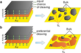
Figure 4. Adhesion balance in the TMDC/Au stack. (a) Scenario, in which the first TMDC layer-Au adhesion is larger than the interlayer adhesion between the TMDC layers, which are all equal. (b) Scenario, in which the first TMDC layer-Au adhesion is larger than the adhesion between the first and second layers of TMDC, which is, however, smaller than the adhesion between the second and third layers.
Download figure:
Standard image High-resolution image2.3. Key factors affecting the exfoliation
The influence of several factors on the exfoliation has been considered. Strain at the interface between 2D material and metal is one of them, as hinted by MoS2 exfoliation on different noble metals [63]. An effective universal strategy towards selective exfoliation of 2D materials, whether prepared by exfoliation or grown synthetically, involves deliberate stressing of the layers to induce interfacial strain [28, 47, 48]. In this case, metals were employed as stressors to fine-tune the balance of the interactions within the layer stack. In one of these studies, a positive correlation was found (but left unexplained) between the number of exfoliated graphene layers and the strength of the interaction between graphene and the deposited metal [48]. Another recent report indicated that the exfoliation process preferentially yields monolayers for unoxidized non-Au metals [52]. The role of strain was disputed by metal-assisted exfoliation of medium-to-large-sized monolayers of MoS2 using Ni, Cu, Ag, and Pd, arguing that the binding energy is the deciding factor [57]. However, Au has one of the weakest binding energies with MoS2 compared to other metals [49]. This implies that a strong binding energy is a necessary condition but not a process bottleneck.
The surface conditions, namely cleanliness, oxidation, and roughness, of the metal substrate, were found to play a crucial role in the exfoliation process [30, 63]. The cleanliness of the 2D material/Au interface has been identified as one of the most important factors for large monolayer yield. The exfoliation proceeds best on freshly grown Au surface and gradually ceases to work after 10–20 min of exposure to air (and longer in vacuum) [30, 64]. This is likely due to the airborne contaminants, which build up on the surface and weaken adhesion between the 2D monolayer and the metal [30, 65]. The exposure of bulk crystals to air is equally critical (although few studies focus on it explicitly), hence, cleavage of the fresh crystal surface must be done as soon as possible before the exfoliation on Au [21]. It has also been demonstrated that sputter-anneal cycling in UHV of an Au surface previously exposed to air can fully recover the strong interaction between TMDCs and Au and enable monolayer exfoliation in air again [66].
Oxidation of the metal has also been shown to be of the utmost importance. While the literature had erupted with studies of 2D materials on Au, exfoliation of large-area monolayer TMDCs on other metals has remained more elusive, with a few notable recent exceptions shown in figures 3(d)–(i) [52, 57]. This is, on the face of it, strange, given the theoretical prediction of stronger binding of non-Au metal to MoS2 [49, 67]. The unique status of gold is the reason for this: unlike other metals, gold does not oxidize, and the MoS2-Au heterostructure appears to be stable upon exposure to air [68]. In contrast, only a negligible amount of monolayer MoS2 is exfoliated after exposure of freshly-grown base metals to air [63]. Slowly oxidizing noble metals do produce some monolayers, however, a few orders of magnitude smaller than on Au.
The roughness of the metal surface leading to weakened TMDC-metal interaction at local depressions has also been proposed to reduce the MoS2 exfoliation yield on Au [30]; however, recent results dispute such conclusions, at least for Ag [52]. The effect of roughness can, to some extent, be compensated by the ductility of the noble metals, which facilitates conformal contact with the TMDC layers [41]. Finally, one study reported that the monolayer MoS2 exfoliation on a template-stripped Au stack was activated only upon thermal annealing to 200 ∘C, believed to be rooted in contamination removal or surface reconstruction [41]. A follow-up study reproduced this behavior for Ag and revealed a maximum in the exfoliation yield at around 150 ∘C due to Ag oxidation at higher temperatures [69].
2.4. Exfoliation on non-Au metals
Several approaches for achieving large-area MoS2 monolayers on non-Au metals have recently been explored. The key is to carry out the entire exfoliation process in an inert environment, i.e. either in an oxygen- and moisture-free glovebox (figures 3(d) and (f)), or, better still, in a UHV chamber (figure 3(e)). The typical partial pressures of oxygen are around 102 mbar in air, 10−5 mbar in a glovebox, and  mbar in UHV. Depending on the rate of oxidation for a particular metal, the typical time windows for successful exfoliation are impractically short in air [63], but could be as long as seconds/minutes in a glovebox [52] or hours/days under UHV [64]. The strong interaction between MoS2 and Ag synthesized under UHV using a pulsed laser deposition was shown to weaken upon formation of substoichiometric molybdenum oxysulfide after the exposure to air [68]. Additionally, Raman and x-ray photoelectron spectroscopy (XPS) helped identify humidity, rather than O2 or N2, as the main cause of surface aging, which was shown to be reversible by UHV annealing at 600 K for 2–3 hours and preventable by covering the surface with a protective polymer layer. In another study, Raman and PL spectroscopy of UHV-exfoliated TMDCs on various substrates showed that the interaction with noble metals Au and Ag is stronger than with base metals Fe and Cr [64]. These authors also exfoliated smaller (10 µm) MoS2 and phosphorene flakes on Au, several days after the metal deposition in UHV. Another recent UHV exfoliation study succeeded in preparing
  m-sized TMDCs on Au, Ag, and Ge, and found that, surprisingly, the Ag substrate yielded somewhat larger flakes than Au [56]. The air-induced degradation has also been suppressed by encapsulating samples with poly(methyl methacrylate) [64, 68].
Metal-assisted exfoliation appears to yield better results (figures 3(g)–(i)) than direct exfoliation, even for base metals, such as Ni [57]. This is consistent with the more abundant evidence for the strong interaction between TMDCs and metals reported for the former approach [70, 71]. We offer the following explanation: during the metal-assisted exfoliation, the individual mobile metal atoms can preferentially bind to available sulfur atoms following the energy minimization principle. The microscopic implication of such a strong interaction is the tearing of the MoS2 monolayer during mechanical peeling of the Au layer from the bulk crystal [62]. This is contrasted by the interaction between the continuous MoS2 flake and metal substrate, in which the atoms are already lattice-bound.
2.5. Transfer to non-metallic substrates
2D monolayers on metals are intriguing systems, rich in fundamental physical and chemical phenomena, and directly applicable to several applied research fields, including optics, catalysis, and energy storage. However, the presence of a metallic substrate, which modulates the properties of the 2D material, is an issue for most other fundamental and applied purposes, namely optoelectronics, photovoltaics, and sensing. Therefore, a reliable method of transferring 2D monolayers from the metal to another, dielectric substrate, such as SiO2, Al2O3, or hBN, or stacking them to large-area 2D heterostructures, is highly desirable. This has been achieved in various ways by several groups [29, 54, 72–74], with the most recent processes allowing to complete the transfer within 30 min [75]. The preservation of the characteristic optoelectronic properties of monolayer MoS2 after transfer from Au to another substrate evidences predominantly vdW, not covalent, character of the MoS2-Au interaction. Clearly, there is a trade-off to be made when designing the 2D/metal stack: the stronger the interaction between 2D material and substrate, the more successful the exfoliation, but the harder it is to remove the metal after transfer. A considerable advantage of the Au-mesh-facilitated dry exfoliation of TMDCs, described earlier, is the elimination of the Au etching from the process [55]. Adjusting the thickness of Au (in the range of 0.1–1.0 nm) also allows one to tune the adhesion strength for a smooth release of a given 2D layer in the assembly of vdW heterostructures [74].
To summarize, a growing body of literature suggests that cleanliness of the interface, interfacial strain, and lack of surface oxidation, are the most important criteria for successful preparation of large-area 2D monolayers on metals, particularly TMDCs on Au. Large binding energy is a necessary but practically unimportant parameter since it is suspected to be large enough for most TMDC-metal systems. Importantly, regardless of the preparation method, and, as long as the interface between the two materials is clean, the strong interaction between TMDCs and metallic substrates significantly affects the physical properties of the system, readily detectable using a range of characterization methods.
3. Fundamentals of the interaction and characterization techniques
3.1. Characterization techniques
Variations in the electronic band structure, lattice constants, and phonon dispersion are typically probed by photoemission spectroscopy, transmission electron or scanning-probe microscopies, or Raman and PL spectroscopy techniques. ARPES resolves the electronic band structure, and XPS provides information on chemical modifications in TMDC layers, e.g. due to defect creation or under the influence of the metallic substrate. Atomic-scale electronic and lattice effects, such as moiré patterns and edge states, can be spatially resolved in STM and AFM. Corresponding changes in the density of electronic states (DOS), e.g. band gap state formation, can be most efficiently monitored by STS or PL spectroscopy. Defect- or substrate-induced lattice deformations and charge/energy transfer effects can be traced using Raman spectroscopy. Influences on the work function and electron affinities can be extracted from KPFM or ultraviolet photoelectron spectroscopy.
While the toolbox of experimental techniques is large, works comparing data from surface-sensitive and optical techniques are scarce: optical measurements are usually done in air, whereas surface-sensitive techniques like ARPES and STM/STS require UHV conditions and surfaces free from ambient contamination. An exception is XPS, which, due to its comparatively large probing depth of 1–2 nm, is often used independently of the sample history [44, 66]. To achieve clean surfaces for ARPES and STM/STS after ex situ handling, samples are usually annealed in UHV at varying temperatures in the range of 100 ∘C–400 ∘C [76]. Such annealing procedures, however, can alter the interfacial properties [77] and also the TMDC itself, e.g. via dichalcogenide vacancy formation, which was reported to start already at temperatures around T = 500 K for MoS2 [77–79]. Respective results from optical and KPFM methods performed ex situ without annealing procedures might therefore reflect a sample in a different status, e.g. with a shifted Fermi level ( ) position. The lack of correlative multi-technique studies represents a bottleneck for a better understanding of the fundamentals of the TMDC-metal interaction.
3.2. Nature of interactions
MoS2 on Au is a good model system to understand the physics of the TMDC-metal interface. Both materials are rather inert to oxidation at ambient conditions, and their electrical, optical, and structural properties are well-studied. Despite this, differing and often contradictory results are obtained by various groups due to differences in the preparation methods and resulting properties of the MoS2-Au heterostructure. Also, researchers have been using inconsistent terminology to describe the nature of the TMDC-Au interaction, adding further confusion to this topic. Various terms, such as strong vdW interaction [30], physisorption or chemisorption [49], covalent-like quasi-bonding [46, 80], or simply strong and weak interaction [44, 66, 81], are commonly used, and boundaries between them are not well defined. Crucially, the interaction strength is on a spectrum encompassing a wide range of binding energies, bond lengths, and changes in the electronic band structure. For example, the binding energy of −0.41 eV per MoS2 (−40 kJ mol−1) [30] between strongly interacting MoS2 and Au is larger (in absolute terms) than the interlayer binding energy of −0.34 eV per MoS2 (−33 kJ mol−1) in bulk MoS2 [30], but significantly smaller than the binding energy of −300 kJ mol−1 in gold monosulfide [82]. Similarly, the separation of 2.9–3.5 Å between strongly interacting MoS2 and Au [30, 49] is shorter than the sum of the Au and S vdW radii (3.9 Å) [83] but substantially longer than the length of 2.2 Å of the covalent Au–S bond in gold monosulfide [82]. Depending on the context of the discussion, we use the terms weak/strong to describe either a vdW interaction inducing a small/large change in 2D material's properties or, in the broader sense, to refer to vdW-like/covalent-like interaction. An example of the former would constitute the stronger vdW interaction between MoS2 and Au versus the weaker vdW interaction between MoS2 on SiO2 or the interlayer interaction in bulk MoS2. An example of the latter would be the vdW interaction between MoS2 and Au, which is weaker than the partially covalent strong interaction between MoS2 and Ni (cf theoretical equilibrium separations of 2.9 Å and 2.2 Å for MoS2-Au and MoS2-Ni, respectively [49]).
3.3. Electronic and transport properties
A strong interaction with partially covalent bonding implies changes in the TMDC lattice and sizable distortions of the electronic band structure, which are not expected for weak vdW bonding. For monolayer graphene, for example, this distinction is clearly reflected in its work function (WF) or vibrational spectra [84, 85] and is wellstudied using photoemission techniques. On the one hand, Dirac states appear deformed and even disrupted in ARPES on strongly interacting substrates like Ru(0001) or Ni(111), reflecting the hybridization of graphene π with metal d states depending on the varying registry of C and Ru atoms visible as moiré patterns [86]. On the other hand, the weak interaction with Au(111) or Pt(111) leads to ARPES features equivalent to an independent superposition of graphene and metal band structures, where graphene bands only shift in energy as a result of charge transfer but otherwise remain undistorted [87]. The weak interaction (13 meV per C-atom) manifests itself also as an absence of structural changes in either material. Even the fragile herringbone reconstruction of the free Au(111) surface is intact under the graphene layer [88] and protected by it from otherwise effective potential-induced transitions [89]. We stress that for each metal substrate, the interaction character can strongly vary with the facet orientation: in contrast to Au(111), the Dirac cone disruption is observed for graphene on Au(001) [90]. The facet-dependent effects also manifest in charge-doping variations and, consequently, in graphene's Raman spectra [91].
According to the literature, covalent admixtures in the bonding of MoS2-Au interfaces seem to always be present along with long-ranged vdW forces, which makes the case less straightforward, compared to graphene. The degree of covalent bonding of MoS2 on Au(111) is, however, far from understood. Density-functional theory (DFT) calculations of MoS2 on perfectly ordered Au(111) predict a predominantly vdW-bonding character. Still, admixtures of covalent bonding vary depending on the assumed strain (which depends on the supercell size) and the choice of DFT functional covering vdW-type interaction [46, 49, 92, 93]. Verification of such DFT calculations on Au(111) is hampered by the fact that most of the experiments on MoS2-Au interfaces have employed inherently disordered Au substrates prepared by magnetron sputtering, electron beam evaporation, or thermal evaporation on Si, SiO2, or mica. Although such films exhibit predominantly (111)-oriented grains, the azimuthal rotation of the grains leads to a polycrystalline in-plane character [94]. These grains also tend to introduce a considerable roughness that makes the MoS2 contact inherently more inhomogeneous as revealed by nanoscale Raman measurements [44].
A large degree of homogeneity can be achieved in bottom-up growth (MBE, PLD) or exfoliation of MoS2 monolayers on UHV-prepared Au(111) single-crystal, exhibiting long-range ordered moiré patterns, which can be modeled by DFT calculations based on periodic supercells. The moiré pattern, visible in STM, evidences a clean and flat interface with a well-defined registry between the MoS2 and Au(111) lattice.
While the bottom-up grown interfaces thermodynamically prefer hexagonal moiré superlattice constants in the range  nm with very small twist angles between MoS2 and Au(111) closed packed directions (Au[
 ] and Au[
 ]) [95–98], exfoliation usually leads to arbitrary twist angles. A typical example for a bottom-up grown moiré pattern at small twist angles (growth according to [98] with a superlattice constant of 3.28 nm) is shown in figure 5(a). Across the twist-angle-dependent hexagonal moiré unit cell, local STS reveals a spatial variation of the MoS2 band gap, suggesting alternating regions of the interfacial sulfur atoms between Mo and Au (Sbottom), with stronger hybridization on top of the Au atoms and weaker hybridization above the Au hollow sites, and respective variations in the extent of covalent bonding. Hereby, the MoS2 layer is commonly believed to remain flat across the moiré [94, 95], although a small out-of-plane buckling by 100 pm in registry with the moiré unit cell and respective strain variations were reported [99]. In XPS, which probes average chemical properties across the moiré unit cells, the strong hybridization of Sbottom atoms becomes visible as a chemical shift in S 2p levels by about 0.3 eV to higher binding energies with respect to the non-interfacial sulfur atoms above Mo (Stop) [100] (see figure 5(b)). It is, however, yet unsettled whether the weakly bonded Sbottom atoms in the Au hollow-site positions might appear unshifted in XPS with respect to Stop, as recently proposed by Silva et al [95]. The presence of strong bonding of the Sbottom is in line with the observations that, unlike for the weakly interacting graphene [88], the Au(111) herringbone reconstruction is lifted underneath the bottom-up grown MoS2 monolayer islands, leaving the MoS2 on either fcc- or hcp-terminated Au surfaces depending on the stacking of the two top Au layers [95, 97, 98, 101].
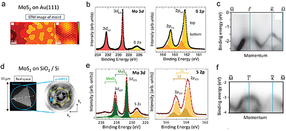
Figure 5. Photoemission spectroscopy of epitaxial 1L MoS2 on Au(111) and bottom-up grown 1L MoS2 on Si-oxide. (a) Hexagonal moiré structure of in situ grown 1L MoS2 on Au(111) (adapted figure with permission from [93], Copyright (2016) by the American Physical Society). (b) XPS core level data of epitaxial 1L MoS2 on Au(111) exhibiting moiré (adapted from [100]. © IOP Publishing Ltd All rights reserved). (c) ARPES data at photon energy hv = 49 eV and T = 80 K [93]. Adapted figure with permission from [93], Copyright (2016) by the American Physical Society. (d) Real space photoemission electron microscopy (PEEM) image and k-PEEM image (0.6 eV below VBM) of a CVD-grown 1L MoS2 island on native Si-oxide. Adapted with permission from [102]. Copyright (2020) American Chemical Society. (e) Respective XPS data. Adapted with permission from [102]. Copyright (2020) American Chemical Society. (f) Room temperature µ-ARPES data at hv = 21.2 eV (adapted with permission from [102]. Copyright (2020) American Chemical Society).
Download figure:
Standard image High-resolution imageDue to the limited spatial resolution, k-space-resolved ARPES data provides band structure information only as a spatial average over many moiré unit cells. Variations in hybridization between 1L MoS2 and Au(111) become mainly visible as distorted and broadened MoS2 valence band states around  , as shown in figure 5(c). The intensity at the upper valence band (VB) around
  is suppressed and the mixing with Au states [93] leads to diffuse and steeply upward-dispersing bands visible in cuts along
  and
and  directions up to
  (the bars above the high-symmetry points Γ, M, and K indicate their definition within the surface Brillouin zone). On the other hand, band curvatures around
  remain less affected by Au. In line with other comparable MoS2-Au works exhibiting moiré patterns [100, 103, 104], the binding energy of the intact
  valence band maxima (VBM) of 1.4 eV corresponds to an
  position just below the conduction band minimum (CBM), suggesting either a certain degree of n-type doping of the MoS2 monolayer, or band realignment effects due to the formation of surface dipoles induced by charge redistributions [67].
The larger susceptibility of MoS2 VB states to Au-bonding at Γ is commonly attributed to an efficient hybridization of out-of-plane S 3pz
and Mo d orbitals with Au 5d orbitals at Γ, versus less hybridizing in-plane Mo 3d
 and Mo 3d
 orbitals at K. The observed distortions in ARPES features around
  can be reasonably well reproduced by DFT, assuming a
  R13.9∘ supercell of MoS2 on a
  Au(111) supercell, enforcing a small 0.15% contraction of the Au lattice [93]. We note that also other supercells with larger mismatches are used in the DFT literature, e.g.
  R30∘ on a
  with approximately 4% mismatch [49, 92]. The respective differences in assumed twist angles also lead to variations in calculated equilibrium MoS2-Au vertical distances of about 0.2 Å [49]. Larger supercells in the range of
  on
on  , which would correspond to moiré superlattices such as the one in figure 5(a), have not yet been calculated due to high computational cost [93].
The trend in bonding behavior and electron band distortions at  has also been reported for CVD-grown monolayer WS2 on Au(111) with evident moiré patterns [105]. The strong bonding effects on gold were also observed for the CDW-exhibiting metallic TMDCs TaS2, NbS2, or NbSe2: the low-temperature CDW formation in 1H-type monolayers is suppressed on Au(111) [106–108]. In a few works, the noble metal substrate was changed to Ag(110) [109] or Ag(111) [105], and a stronger interaction of 1L MoS2 and WS2 was reported due to a more efficient hybridization between Ag bulk bands and the TMDC's conduction band states. For Ag(111), ARPES shows the filling of CB states near TMDC
  points, located along the Γ-K directions, attributed also to the lowered surface work function compared to Au(111) [105]. The occupation of CB states triggers a semiconductor-to-metal transition in the TMDC, which enhances dielectric screening and significantly reduces excitonic effects in optical absorption processes [110].
In contrast to the discussed metal (111) and (110) surfaces, ARPES band distortions are much weaker for 1L MoS2 flakes on weakly interacting Si-oxide or graphene [112, 113]. Figure 5(d) and (f) shows typical µARPES data for a bottom-up grown 1L MoS2 flake on SiO2. Corresponding XPS spectra are shown in figure 5(e). The XPS and ARPES features in (e) and (f) are considerably shifted to higher binding energy with respect to data on Au(111). This shift is partly due to sample charging during photoemission on the non-metallic SiO2 substrates, which makes, e.g. absolute values of XPS peak positions in (e) unreliable. Due to the limited conductivity of the SiO2 substrate, ARPES has to be performed at higher temperatures, which contributes to the general broadening of features compared to low-temperature data on metal substrates, e.g. that of figure 5(c).
For 2D semiconductor-metal interfaces, so-called metal-induced gap states have been reported to cross the band gap in MoS2 on Au(111) [77], often also referred to as interface states [49, 93]. However, according to DFT, another gap state type is predicted to exist due to the hybridization of the interface S atoms with Au [67]. The interfacial Au-Sbottom bonding weakens the Sbottom-Mo bond, due to which the band edge states (composed mainly of Mo d-orbitals) spread into the band gap, appearing as a diffuse DOS of Mo d-orbital character in the gap region in figure 6(c) (red curve). The prominent spreading of states into the gap is not observed for 1L MoS2 on Si with a native SiO2 [112], where the energy dispersion remains similar to that of freestanding 1L MoS2, as shown by the DOS-energy dependence in figure 6(b).
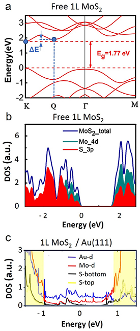
Figure 6. Band structure and density of electronic states. (a) Typical calculated band structure of a freestanding 1L MoS2 in the high-symmetry Γ-K and Γ-M directions with the direct band gap at K (adapted from [111]. CC BY 4.0). Along the Γ-K direction, a local minimum is visible at the Q point in the conduction band. The energy difference with respect to the CBM at K is marked by blue arrows. (b) and (c) show DOS calculations for freestanding 1L MoS2 (adapted from [111]. CC BY 4.0) and 1L MoS2 on Au(111) with partial sulfur and molybdenum contributions (adapted with permission from [67]. Copyright (2014) American Chemical Society). In (c) also, the Au DOS is plotted, and the sulfur contributions are further divided into Sbottom (with Au-contact) and Stop (non-contact).
Download figure:
Standard image High-resolution imageGap states play a pivotal role in the physics of the metal-semiconductor interface as they are responsible for the Fermi level pinning, which affects transport properties and the work function of the material [66, 67, 114]. When a metal and a semiconductor are in contact, their Fermi levels equalize, and, according to the Schottky–Mott rule, the Schottky barrier height (φB) should depend only on the work function of the metal and the electron affinity (χ) of the semiconductor. In MoS2-metal systems, φB
deviates from the Schottky–Mott rule due to  pinning [62, 114]. The metal deposition techniques introduce defects, strain, and impurities responsible for the appearance of gap states and interface dipoles [62]. The presence of gap states and the formation of an interface dipole modify the metal WF and pin the
  up to a few hundred meV below the CBM [16, 114]. Taking into account reported direct band gaps of 1.9 eV or 2.1 eV [115, 116] at K, this is in line with ARPES data, e.g. in figure 5(c), where the VBM at
  appears at the binding energy of about −1.4 eV. The proximity of
  to the CBM explains the typical n-type field-effect behavior for MoS2 in transport measurements [16, 114]. In MoS2, n-type doping is observed regardless of the work function of the metal when it is deposited directly on the surface, while for MoTe2, strong p-type doping was observed [62, 114, 117]. The contact resistance varies by orders of magnitude (from GΩ to kΩ) even when the same metal and deposition technique is used, but aligning the metal work function with the TMDC CBM or VBM usually reduces the contact resistance in FET devices [117–119]. DFT shows that when the TMDC is pulled away slightly from the metal surface, the partial covalent bonding is suppressed, and the band alignment obeys the Schottky–Mott model [67]. Interfaces free of
  pinning and contacts with low φB were achieved experimentally by transferring metal films with work functions that match the CBM or VBM of MoS2 [62], while φB can be completely reduced, thereby achieving ohmic contacts by using Bi and In as the contact material [120, 121]. The Schottky–Mott model also predicts band-bending to occur on the semiconductor side in the metal-semiconductor interface, which was experimentally verified for MoS2 in contact with graphene [122] and for MoS2 line defects and edges [123]. Still, no such bending was observed at the interface of a metal and highly doped MoS2 [124].
Most data on metal-semiconductor junctions were obtained through transport measurements or STM/STS measurements on samples with highly oriented interfaces [81, 114, 120, 124, 125]. Similar information can also be obtained by KPFM even under ambient conditions [51, 66]. For bulk layered materials, the top surface is far from the inner interface with the metal, and, therefore unaffected by it. In directly exfoliated samples, however, the effects of the metal-2D material interface can be 'felt' through the monolayer and therefore accessed experimentally even by surface-only sensitive methods. Pollmannn et al approximated the measured WF to be the sum of φB and χ, reasoning with the extremely small thickness of the TMDC monolayer [66]. However, this assumes that no equivalent of band bending or unexplored spatial quantum effects occur in the TMDC monolayer, which remains to be investigated experimentally. MoS2 monolayer exfoliated on Au was found to be relatively p-doped compared to transferred CVD MoS2, which is assumed to be n-doped [66]. Due to the predicted strain and band gap renormalization in the TMDC-metal system, the evaluation of KPFM measurements is not straightforward and changes in the electron affinity, ionization energy, and the band gap need to be considered when determining the φB and the type of doping [16, 49, 51, 126]. Moreover, the layer-dependent nature of the band structure needs to be taken into account for multilayer materials. Another possible interpretation of the KPFM measurements was proposed by Jo et al, where the interface dipoles are the dominant contributors to the contact potential difference measurements in KPFM due to the insufficient thickness of a MoS2 monolayer to screen the interface dipole potential [51]. For MoS2 directly exfoliated on Au, the WF was lower (5.05 eV) than that of Au (5.16 eV) as shown in figure 7(a). Although this indicates that positive charges accumulate on the MoS2 side, it maintains the n-type semiconducting character as the Fermi level is still closer to the CBM than to VBM [51].

Figure 7. KPFM, Raman, and PL characterization of MoS2 on metals. (a) Contact potential difference map of MoS2 directly exfoliated on Au. The scale bar is 1 µm. (Adapted with permission from [51]. Copyright (2021) American Chemical Society). (b) Comparison of the Raman spectra of MoS2 directly exfoliated on Au and SiO2 (adapted from [44]. CC BY 4.0). Shift of the E mode and the splitting of the A1 mode are typical Raman fingerprints of the strong interaction. (c) Strong quenching of the PL of 1L MoS2 directly exfoliated on Au (red) compared to suspended MoS2 (black) and MoS2 exfoliated on SiO2 (green), and the signal of bare Au (blue) (authors' results). (d) Raman spectra of 1L MoS2 directly exfoliated on different metals showing different degrees of strain (adapted from [63]. CC BY 4.0). (e)–(f) Raman and PL spectra of 1L MoS2 directly exfoliated on different metals in UHV (reprinted from [64], Copyright (2022), with permission from © 2022 Science China Press. Published by Elsevier B.V. and Science China Press. All rights reserved).
Download figure:
Standard image High-resolution imageFew studies of MoS2 on Au(111) simultaneously confirm the moiré pattern using the surface-sensitive STM and characteristic changes in the ex situ Raman and PL spectroscopy [97, 127]. Tumino et al reproduced the STM patterns in UHV after optical measurements in air to verify sample stability [97], which is in line with earlier air exposure tests reported in [98]. The characteristic changes in Raman and PL spectra, absent for 1L MoS2 on SiO2 or graphene [128, 129], are considered a reliable optical signature for strong vdW character of the bond between MoS2 and Au(111) and respective strain variations in the presence of a moiré structure [99]. We stress that the specific periodicity of the moiré pattern in [99] cannot play a key role in the strong vdW interaction. This is because similar strong changes in Raman spectroscopy and missing PL have also been observed for 1L MoS2 on less ordered magnetron-sputtered, e-beam evaporated, and thermally evaporated Au substrates [44], where the moiré pattern is not observed due to the large roughness and small grain size of Au. Nevertheless, a recent study demonstrated that samples with large moiré superlattice wavelengths originating from small twist angles ( ) show larger changes in the electronic structure of MoS2 and stronger charge doping [94].
3.4. Optical fingerprints of the strong interaction
Till now, no correlations were found between the moiré pattern and the Raman and PL measurements for the strongly interacting MoS2 on Au(111). The interpretation of the interaction-induced changes in TMDC Raman spectra, in particular the shifts of the in-plane E and out-of-plane A1 modes and the appearance of new peaks, is usually discussed in terms of strain, charge-transfer, and symmetry-breaking effects in the TMDC layers [130]. For 1L MoS2, the symmetry point group is reduced from D , when suspended, to C
 , when exfoliated on a metal substrate. Therefore, the notation changes from E
 and A
and A for bulk, to Eʹ and A
 for suspended or weakly interacting monolayer, and to E and A1 for strongly interacting monolayer [128]. Measurements also show that only the first layer, directly in contact with the Au surface, is strongly interacting with it [44, 66]. This observation corroborates the exfoliation mechanism proposed in figure 4(b).
A clear fingerprint of the strong interaction between monolayer MoS2 and Au is the activation of the symmetry-forbidden A1 mode at 455 cm−1 (A notation in bulk) and the geometry-forbidden mode E mode (for back-scattering setups) at 280 cm−1 (E
 in bulk), predicted by group theory and confirmed experimentally [30, 66, 81, 96, 128]. We note that due to the symmetry considerations, the newly activated modes now have the same notation (symmetry) as the normal modes commonly associated with MoS2. To avoid confusion, in the following, the E and A1 notation will explicitly refer to the normal modes (i.e. E
 and A
and A in the bulk notation), unless stated otherwise. In line with DFT, the forbidden modes appear only in MoS2 strongly interacting with Au but are absent in freestanding MoS2 and MoS2 on weakly interacting SiO2 substrate. Still, the main Raman fingerprints for strong MoS2-Au interaction with Au(111) substrates are the downshift of the E mode and broadening/splitting of the A1 mode with respect to monolayer MoS2 on SiO2/Si, shown in figure 7(b), indicating the possible presence of an in-plane tensile deformation and charge transfer in the MoS2 lattice [44, 66, 131–134].
The downshift of the E mode of MoS2 on Au (unstrained at ∼386 cm−1) corresponds to 1%–3% of biaxial tension [44, 135]. The E mode also broadens, and, in some cases, a second component can be seen as a shoulder peak [44], possibly due to the variations in the twist angle between MoS2 and Au lattices or the coexistence of MoS2 regions conformal to and suspended between Au grains. Uniaxial strain might be another potential cause of the E mode splitting, as the double degeneracy of the E mode is lifted due to the change of the point group symmetry as a result of anisotropic deformation [136]. In contrast, the degeneracy is preserved for biaxial strain and the E
 mode only shifts [135]. A broader and more asymmetric E mode is observed for MoS2 on some non-Au metals (Ag, Pt), see figure 7(d), where spatial heterogeneity could be linked to the larger susceptibility of these metals to oxidation [63]. Importantly, the position of the E
 mode does not change considerably when the material is charge-doped [129, 137, 138].
In contrast, the observed splitting/broadening of the A1 Raman mode of MoS2 on Au was attributed primarily to electron doping [44]. The A1 mode splits into two components, A1(L) and A1(H), as shown in figure 7(b) [44]. After correction for the strain, the downshift of the A1(L) mode suggests significant n-type doping, while the upshift of the A1(H) mode suggests slight p-type doping. This analysis was based on earlier studies, which showed that the A1 mode downshifts and broadens for electron doping but changes negligibly for hole doping [129, 133, 134, 138]. For clean samples, n-doping (p-doping) can be observed as shifts of the VBM to higher (lower) binding energies in photoemission measurements. The n-doping can also be induced purposefully by deposition of potassium atoms, which push the  into conduction band states at
  [113].
Furthermore, tip-enhanced Raman spectroscopy (TERS) has shown that, within a few nm lateral resolution, the A1(L) and A1(H) modes appear individually and are mutually exclusive to the parts of the MoS2 lattice with strong and weak interaction with Au [44, 128]. The binary character of the A1(L) and A1(H) modes is further corroborated by variable-force TERS measurements of a transferred MoS2 monolayer on a gold substrate with a thin layer of contamination. Moreover, the weak MoS2-Au interaction for a contaminated interface locally strengthens with the increasing tip force, which is reflected in the appearance and increasing intensity of the initially absent A1(L) mode, concurrently with decreasing intensity of the A1(H) mode [44, 128]. DFT supports the measurements as the A1 mode should only be shifted in the strongly interacting MoS2 [92, 128]. However, a clear explanation of why the splitting is observed only for the A1 mode, and not for the E mode, is missing. One would, in fact, also expect the interaction strength to be locally reflected in differences in the MoS2 in-plane lattice deformation [92]. One possible reason is the disparity between the continuous propagation (relaxation) of strain levels [139], causing a broad and mostly symmetric E mode, and the more delimited nature of charge-doping [128, 140], akin to graphene on Ir [141], or Mo-S bond weakening [66], responsible for the discrete splitting of the A1 mode.
Despite the evidence for n-doping of MoS2 on Au, some KPFM measurements hint at p-doping instead [66, 142]. However, the band gap renormalization, changes in χ due to the hybridization between Au and MoS2 orbitals, and the layer-dependent nature of the band structure were not considered, and therefore, the results are inconclusive. Irrespective of the doping, the splitting of the A1 mode can also be explained as the weakening of the Mo-S bond due to the interaction with Au [44, 66, 127]. The shifts of the Mo 3d and S 2p
 peaks to lower binding energies are also interpreted as heightened oxidation states of the atoms due to bond weakening [66]. Another theoretical explanation of the downshift of the A1 mode involves the spill-over of the electronic charge into the MoS2 conduction band [92], which is lowered due to strain and becomes partially populated as it falls below the
  of the system. As discussed above, ARPES measurements of MoS2-Au(111) with moiré pattern indeed show that the VBM usually appears at binding energy of about 1.4 eV (see also figure 5(c), suggesting that the
  is just below the CBM [113].
Although most of the authors agree that the downshift of the E mode is due to tensile strain and the splitting of the A1 mode is due to charge transfer, a definitive answer to the origin of these changes requires more experimental evidence. Interestingly, some STM studies conclude there is no significant in-plane lattice deformation of MoS2 [97, 98], which would rule out tensile strain as the cause of the E mode downshift. However, the smallest reported measurement error in these studies is equivalent to ±1.6% of strain [97], larger than the average tensile strain determined from the Raman spectra [44]. Furthermore, differences in strain magnitude and distribution likely exist between the bottom-up grown MoS2 and the top-down exfoliated MoS2, with the former being allowed to relax during the growth process in contrast to the latter with a forced lattice mismatch between MoS2 and Au. The underlying mechanism governing the shifts of the E and A1 modes depending on strain and doping may be more complex when considering the particular electronic structure of MoS2.
The conduction band states in monolayer MoS2 originate primarily from the Mo 4 orbital at the K point and Mo 4
 orbital halfway between the K and Γ points [143]. The former has the same symmetry as the A1 mode and, thus, a population of these states influences the downshift of the A1 mode [92, 133]. Because the symmetry representation of the E mode is orthogonal to the symmetry representation of A1, the E mode is not affected, which is comparable with other theoretical predictions and experiments [92, 133]. The splitting of the A1 mode is then explained as the coexistence of the strained and unstrained models [92].
Another theoretical study predicted the downshift of the out-of-plane mode to occur only when charge carriers occupy multiple nonequivalent valleys [134]. As the band structure changes with strain and/or hybridization, it could affect the population of the conduction (valence) band during electron (hole) doping, which could, in turn, influence the shift of the out-of-plane mode. The authors argue that this is the case for MoS2 where the downshift of the A1 is correlated with the charge occupation of multiple valleys, which in turn increases the strength of the electron-phonon coupling due to reduced effectiveness of charge screening [134]. K and Q valleys in the conduction band are good candidates for co-population, as their energy separation (ΔE) tends to be small for 1ML MoS2 as indicated in figure 6(a).
Experimentally, a shift of the CBM from K to Q was so far not reported for MoS2 or WS2 on Au(111) systems. However, as mentioned above, ARPES studies showed that it is the case for bottom-up grown WS2 monolayers on Ag(111) substrates, for which  moves into conduction band valley at
  [105]. In XPS, the metallic character of WS2 becomes visible as shifted and asymmetric W 4f core level shapes, which is assigned to enhanced core hole screening. DFT theory of freestanding tungsten-based TMDCs predicted that K and Q valley energy separations could vanish, e.g. at uniaxial compressive strains in the range from 0.5% to 1.5% [144]. However, the analysis of the surface moiré pattern on Ag(111) in [105] rules out strains larger than ±0.7%. Moreover, from the slightly larger lattice constant of Ag(111) compared to Au(111) it is unlikely that the effect is mainly driven by an increase in WS2 compressive strain. Despite the interest, respective ARPES measurements of MoS2 on Ag(111) are missing. ARPES data on bottom-up grown MoS2 monolayers on Ag(110), however, exists, showing again a semiconductor-metal transition and a shift of the CBM from
  to
to  with anisotropic stretching of the MoS2 lattice vector along Ag[1
 0] by 3% [109].
We want to stress that, in some cases, the large area exfoliation is not accompanied by the Raman spectroscopy fingerprints detailed above [46, 81, 145]. In these studies, only slight or no shifts in the Raman modes were observed, and PL was present, albeit lower in intensity, compared to MoS2 on SiO2 due to quenching. The analysis of the PL, therefore, cannot be utilized to aid in resolving the discussion regarding the strain and charge levels, as is commonly done for MoS2, e.g. on SiO2 [129, 135], due to charge-transfer-induced quenching on Au, figure 7(c) [30, 66]. Conversely, the complete lack of PL serves as another optical fingerprint of strong interaction in the TMDC-metal system. A PL signal, which is still preserved in MoS2 transferred onto Au [66], testifies to the need for having both the metal substrate and the bottom side of the TMDC fresh and free of contamination to induce their strong interaction upon the touch.
3.5. Beyond the MoS2-Au system
The large-scale exfoliation and changes of optoelectronic properties are not limited only to the MoS2-Au system. Up to now, more than 40 layered materials were successfully exfoliated on e-beam evaporated Au [46]. Figure 7(d) shows the various downshifts of the Raman E mode of MoS2 exfoliated on Au, Ag, Pt, and Pd, which were assigned to tensile strain [63]. Larger strain values were positively correlated with the monolayer lateral size, suggesting that strain plays an important role in the exfoliation yield. Although exfoliation on other metals in air proved to be difficult due to surface oxidation, Heyl et al [69] exfoliated millimeter-sized flakes of MoS2 on Au and Ag by heating the substrate. Raman spectroscopy suggested a heterogeneous strain of MoS2 on Ag seen as the splitting of the E mode, which is more pronounced at higher temperatures, probably due to increased oxidation of Ag. The heterogeneous strain could be due to the formation of Ag nanoclusters as the strain is distributed locally along the MoS2-Ag boundaries and is highly inhomogeneous [71].
To prevent surface oxidation, exfoliation must be done in a glove box or under UHV [52, 56, 64]. In one such study, up to 12 materials were exfoliated on Ag inside a glove box [52]. The PL was quenched for samples exfoliated on a smoother Ag surface, while enhanced PL due to surface plasmon-polariton and localized-surface-plasmon-resonance was observed for MoS2 and MoSe2 exfoliated on a rougher Ag surface [52]. Medium to large (∼100 µm) flakes of MoS2, WS2, WSe2, and WTe2 were also exfoliated on Au, Ag, Fe, and Cr surfaces in UHV [56, 64]. In the case of WSe2 on Ag(111) and WS2 on Au(111), the ARPES revealed hybridization of out-of-plane orbitals indicating at least partial chemisorption [56].
In the case of MoS2 exfoliated on Au and Ag in UHV, its Raman spectra had characteristic fingerprints for the strong interaction [64]. In contrast, on Fe and Cr, the spectra are similar to suspended monolayers, indicating a weaker interaction. This is also evident in the PL spectra, as the PL is quenched only on Au, and redshifted for other metals compared to suspended MoS2 [64].
4. Challenges and applications
Despite the tremendous surge of interest in exfoliated 2D materials on metals in recent years, preceded by studies of graphene deposited on or covered by metals, there are still many open questions concerning the intimate interactions between the respective counterparts, both from the fundamental point of view and application perspective.
The controversial debate on the fundamental understanding of the interaction itself is fueled not only by the lack of a broader range of experimental data, including different TMDC-metal combinations, but also by limited reproducibility even for well-studied systems like MoS2 on Au. This starts right with the preparation of the interface: purity of the metal and 2D crystal, metal surface roughness, time between metal deposition and exfoliation of the 2D material on top of it, time between the exfoliation of fresh 2D surface and metal deposition on top it, the content of oxygen, moisture, and impurities in the surrounding medium, post-exfoliation annealing temperature, sample storage etc. The discrepancies continue with the characterization. One example is the laser excitation wavelength for Raman spectroscopy, where only results obtained by the same excitation for a particular TMDC can be mutually compared, as each wavelength brings forth distinct exciton-phonon coupling and resonance effects [128]. More complicated issues arise during KPFM measurements, where incorrectly chosen tip-standard combinations, large differences in ambient humidity, or contamination on top of the 2D material can all shift the obtained work function by hundreds of meV [146, 147]. Surface roughness, contamination, or defects can, in turn, also affect the photoelectron emission spectroscopy measurements as an independent method to detect work function changes. The role of defects is complex and influential in various aspects of the 2D material-metal contact. Vacancies in the top-most Au layer are predicted to locally modify the S -Au bonding [92], Mo-vacancies and Mo-substitutional defects induce strong
  pinning and reduce the φB at the MoS2-metal interface [148], and, to add to the confusion, different kinds of defects induce different doping character [149]. From the theoretical side, predictions by the DFT also suffer from unsettled methodologies, which generate divergent results. Theorists use different functionals, model supercells of varied sizes affecting the lattice mismatch, and employ various combinations of TMDC and metal relaxations at different stages of modeling the superstructure, all of which generate divergent results [30, 49, 67, 92, 105, 150]. These factors have to be assiduously considered before interpreting and debating the collected data.
One of the main puzzles is the state of the TMDC on top of the metal. Some controversies stemming from the different views on the origin of the E and A1 Raman modes of MoS2 on Au have been discussed. Why do neither the STM [97] nor the XRD [61] measurements show larger strains, which would correspond to the theory [49, 92] and experimental Raman E mode downshift [44, 66]? Similar to what was proposed as the cause for the A1 Raman mode downshift, i.e. a modification of Mo-S bond strength [66], one could investigate changes in the charge redistribution, short- versus long-range interactions, or the dielectric tensor as possible reasons for the E mode variations. Such changes in substrate-induced bond length variations have been addressed by several photoemission studies, however, with varied experimental results and contradictory interpretations. Observed chemical shifts and characteristic asymmetric core level line shapes in XPS are interpreted as heterogeneous coordination states of sulfur (e.g. S
 versus S
 , or weakly versus strongly interacting areas of MoS2 on Au) [44, 66, 100]. Nevertheless, interface charge-transfer processes can also explain asymmetric peak shapes and energy shifts, when
  is shifted, and the metallicity of TMDCs increased [105]. Shifts in
  can, in principle, be directly proven by ARPES, however, respective experimental data is often not available as sample surfaces lack the necessary cleanliness.
Important clues can be found in the systems with other metals, which show different E mode shifts, splitting, or asymmetry [63, 69]. Even more controversies surround the roots of the A1 mode downshift, which can be, at a first glance, assigned to n-doping based on previous studies of electrostatically gated 1L MoS2 [129, 133, 134]. Such a large downshift of almost 6 cm−1 (corrected for the possible in-plane strain shift) would mean a very high electron density of  cm−2 [44], which is somewhat surprising for a 'static' charge doping by a substrate. In contrast, some KPFM results show a p-doped character of MoS2 on Au [66, 81]. However, the
  obtained from KPFM may too suffer from the measurement conditions and the higher absolute
  value can, in part, be attributed to tensile strain, according to DFT [151].
Another open question concerns the potential phase transition of the TMDC from the thermodynamically stable 1H to the unstable 1T or 1T' polytype in the presence of a strongly interacting substrate. Theory predicts charge doping as a mechanism of lowering the energetic barrier of transforming the 1H to 1T phase, which is otherwise energetically unfavorable based on the formation energy comparison of the three polytypes (1H - 80 meV/atom, 1T - 360 meV/atom, 1T' - 270 meV/atom). Several authors suggested [96, 152, 153], based on STM observations of local changes of the moiré pattern, STS showing a vanishing band-gap, or Raman spectroscopy, that the 1H phase of MoS2 on Au can locally change to 1T/1T'. Nonetheless, interpreting these results should also be considered from different perspectives. First, the existence of different adjacent moiré patterns, interpreted as the existence of adjacent 1H and 1T regions in MoS2 exfoliated on Au (figure 8(a)) [96], most likely originates from the relative rotational misalignment of the Au single-crystal grains underneath the ordered 1H MoS2. Indeed, directly adjacent regions with different moiré patterns but continuous MoS2 lattice across the moiré boundary were reported in different works (figure 8(b)) [94, 97]. Second, the position of Raman J1–J3 peaks (figure 8(c)), which are proposed as evidence for the presence of 1T/1T' phase in [96], does not correspond to previous reports [154], where the phase transition was achieved through pressure [155] (figure 8(d)) or lithium intercalation [156]. Third, the STS showing the metallic character of MoS2 on Au may also not be a clear evidence of the phase transition, as the metallicity is also expected from the hybridization with Au orbitals while the 1H phase of MoS2 is preserved [30, 77]. In the same vein, metallicity observed in WS2 on Ag was attributed to strong hybridization between the electronic bands of both materials and the 1T phase existence was conclusively ruled out by photoemission spectroscopy [105]. Annealing to 500 ∘C or He-ion irradiation was also shown not to induce the phase transition [157]. In some instances, though, when tuning the MBE growth conditions of MoS2 on Au, quick temperature quenching was shown to preserve more of the 1T phase in contrast to slow cooling where the 1H phase is preferred [153].

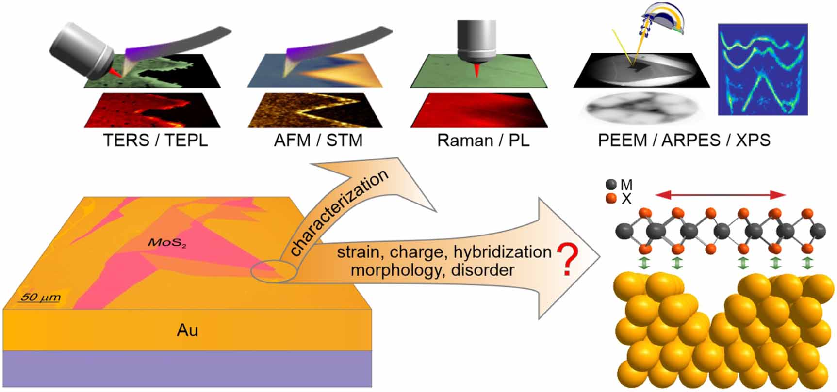
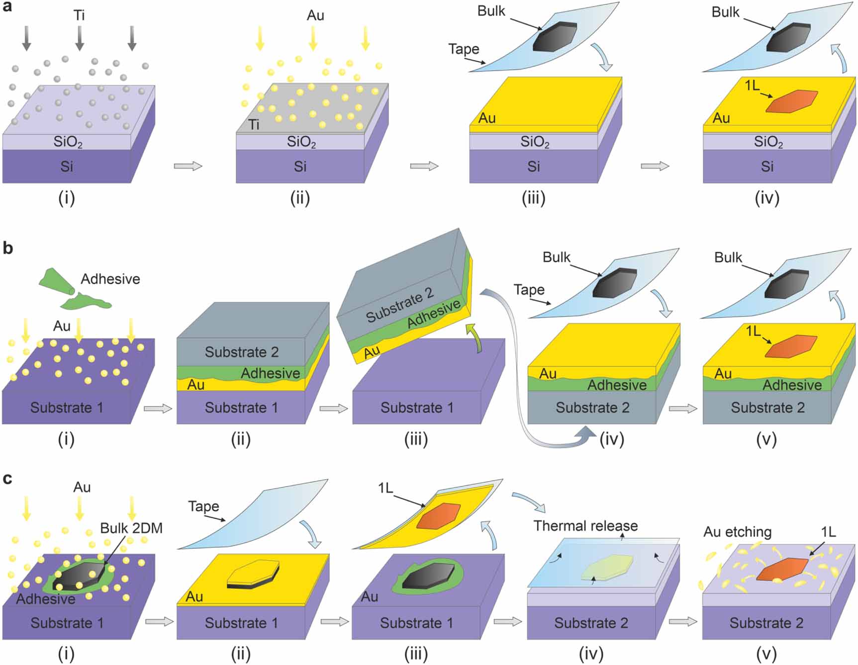
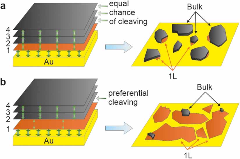
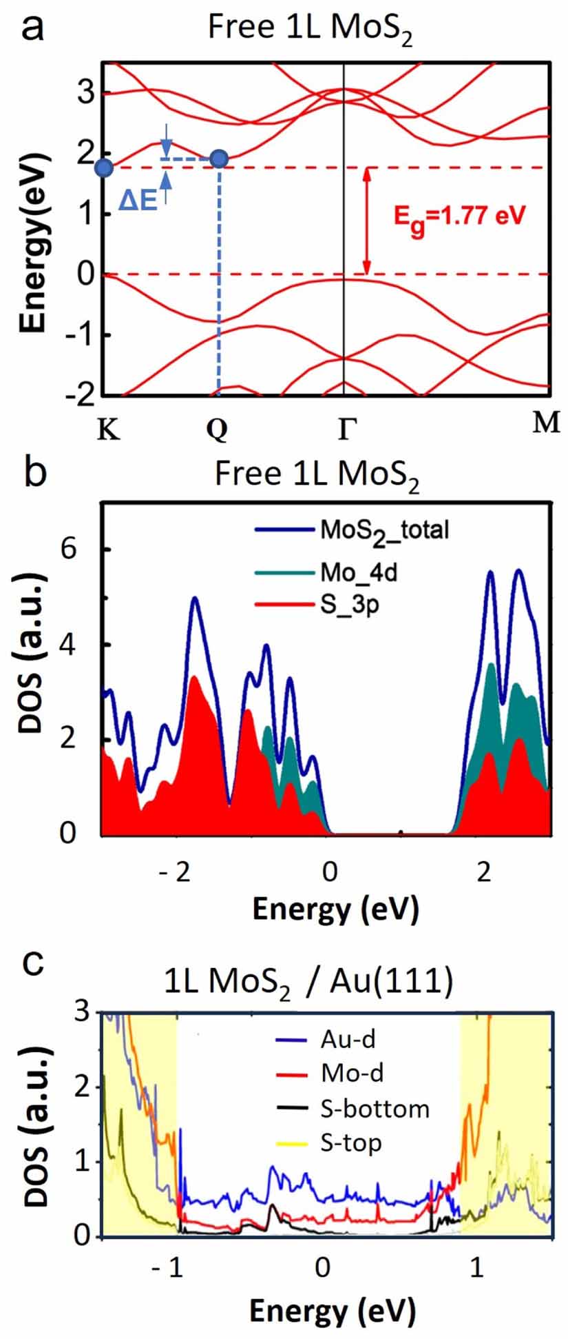
Figure 8. 1H vs. 1T' phase. (a) STM image of 1L MoS2 directly exfoliated on Au. Two regions with different patterns were observed; one was assigned to the 1T phase (adapted with permission from [96]. Copyright (2020) American Chemical Society). (b) STM image of 1L MoS2 crystal growing over an Au(111) boundary. Labels α and β denote two different moiré patterns (adapted with permission from [97]. © The Royal Society of Chemistry 2019. CC BY-NC 3.0). (c) Raman spectra of 1L MoS2 directly exfoliated on Au (orange) and bulk MoS2 (green) (adapted with permission from [96]. Copyright (2020) American Chemical Society). (d) Raman modes for the pressure-restacked monolayer 1T'-MoS2 (black), monolayer 2H-MoS2 (red), and multilayer 2H-MoS2 (blue) (Adapted with permission from [155]. Copyright (2014) American Chemical Society). The position of the J1–J3 modes does not coincide in (c) and (d).
Download figure:
Standard image High-resolution image
The 1H to 1T phase engineering is appealing not only from the fundamental physics point of view but also as an efficient improvement of the contact resistance in TMDC-based devices, as the metallic 1T phase forms an ohmic contact to the metal [156]. Nonetheless, one does not need to rely only on the metallic 1T phase in contact engineering. Variable Schottky barriers and ohmic contacts at room temperature can be achieved by transferring metal electrodes onto 1H TMDCs [62, 158]. In contrast to the transferred electrodes, directly deposited metal contacts produce near-constant φB due to the formation of defects, which pin  near the CBM of MoS2. Ohmic contacts with near-zero Schottky barriers due to the suppression of the gap states have been achieved using bismuth even for temperatures below 100 mK [118, 120].
In this vein, the fundamental studies of 2D material-metal interactions are immediately connected with relevant applications. The strong interaction leads to the exfoliation of high-quality large-area monolayers, which have been challenging to fabricate before the birth of the metal-mediated exfoliation techniques. With established methods of transferring the large-area 2D monolayer to arbitrary insulating substrates [54, 75], the field of optoelectronics is now open to numerous possibilities for applications, where the lateral size of the monolayers has previously been limiting. Novel approaches, such as utilizing the selective and quantitative monolayer exfoliation for patterning and vdW heterostructure assembly, have exploited these features [72, 159].
5. Conclusion and outlook
The integration of metals into the exfoliation and growth processes of 2D materials has ushered in a new era, revealing a multitude of interaction types and resulting properties of these complex systems. High-quality, large-area samples of 2D materials on metals are accessible to a wide range of characterization methods, whose use has been limited by the small size of the monolayers to date. The metal-mediated exfoliation methods are very robust and, as we describe in this review, the parameters controlling their efficiency are now well understood. Beyond the purely scientific interest in the fundamental nature of the 2D material-metal interaction, this research area holds the key to transformative advancements in applied (opto)electronics, where high material quality, scalability, and tunability are highly important.
As we navigate this captivating landscape, fundamental questions emerge, especially concerning the state of the TMDC atop the metal substrate. We delve into controversies, such as the changes in Raman signatures of MoS2 when interfacing with Au, and present potential explanations. We explore the interplay between charge redistribution, substrate-induced bond length variations, and the intricacies of interface charge-transfer processes. Furthermore, we consider the prospect of TMDC phase transitions induced by the strong interaction with the metal.
Despite the recent surge of interest and the growing body of research, critical gaps in understanding the intricate 2D material-metal interfaces persist. In our closing remarks, we offer insights into the challenges that lie ahead, urging for continued exploration to unravel the complexities of TMDC-metal interactions, which have the potential to pave the way for transformative advancements in nanoelectronics and beyond.
Acknowledgments
L P, J H and M V acknowledge the funding support by the Czech Science Foundation Project No. GA22-04408S. The study was also supported the Czech Academy of Sciences Lumina Quaeruntur Fellowship No. LQ200402201 and the European Regional Development Fund; OP RDE (Project No. CZ.02.1.01/0.0/0.0/16_026/0008382). We thank Michaela Hanušová for preparing (and taking the image of) the sample in figure 3(d).
Data availability statement
All data that support the findings of this study are included within the article (and any supplementary files).
Author contribution
The manuscript was written through the contributions of all authors. All authors have approved the final version of the manuscript.