1. Introduction
Polydimethylsiloxane (PDMS) is a silicon-based elastomer, characterized by its high elasticity, good optical transparency, biocompatibility, thermal stability, chemical inertness, and low autofluorescence. Its good elasticity depends on the siloxane (Si-O) backbone, which in this context is better than the carbon (C-C) one present in other polymers. Owing to its elasticity, easy moldability, large elastic limit, fast recovery from high and frequent deformations, and durability in harsh environments, its surface can be functionalized.
PDMS appears promising as an elastic substrate because it can easily adjust to the soft tissue curvatures in biomedicine. Its chains are chemical crosslinked by covalent bonds and its mechanical features can be tuned, changing the amount of the curing agent or the crosslinking temperature [
1]. One drawback of using PDMS for biomedical applications as joint implants or culture cells is its hydrophobicity with aqueous solvents due to the presence of methyl groups [
2]. However, its hydrophobicity can be converted to obtain adhesive surfaces, since the PDMS surface physical properties, such as roughness and morphology, greatly influence the wettability and the adhesion of active materials.
At present, there are two routes for the fabrication of stretchable electronic devices: (1) the active materials such as metals and semiconductors with the desired electrical properties are laid on an elastic substrate (PDMS); (2) the elastic substrate (PDMS) becomes stretchable conductor/strain sensors after mixing with conductive nanomaterials [
3]. Under stretching of the substrate, the strain on the active materials will be dissipated by the structures, which can be previously realized or spontaneously formed (i.e., mechanically).
Typically, a material’s surface modification indicates altering of the surface properties of a material to enhance its specific functions, preserving the bulk features; this goal can be attained by fabricating a thin film on the material’s surface. Pulsed laser deposition (PLD) and laser-induced backward transfer (LIBT) can be used for this purpose. The former technique is more suited to free oxidizing impurities deposition for dental and orthopedic prostheses and in vitro studies involving fibroblasts and osteoblasts, providing excellent adherence and biocompatibility of the deposited material [
4]. The latter one is used to realize particular patterns on the material’s surface. In fact, beside the production of biomaterial thin film for tissue engineering, localized spatial organization of proteins and cells [
5] is gaining wide interest for the study of the interaction between cells and substrates to pilot cell growth along appropriate directions in the fabrication of implants or biosensors.
Despite plenty of techniques are applied to modify the PDMS surface, such as triggered surface activation [
6], oxygen plasma surface activation, chemical gluing, and mixed techniques [
7], this paper will focus on the use of the above cited two techniques—PLD and LIBT. PLD is an established, fast, and controlled deposition approach that can be performed in vacuum [
4], in air [
5], in gases [
8], and in liquids [
9]. LIBT is usually carried out in air. Of course, during these processes, the laser fluence, wavelength, pulse duration, and the ablation environment play a key role. Therefore, both PLD and LIBT can lead to the desired modification of the PDMS.
Adly et al., in their study, refer to the realization of carbon high-resolution patterns with complex electrode geometries on PDMS by ink-jet printer. Carbon was chosen because of its electro-chemical stability, low impedance for electrical sensing, and stimulation of cellular activity compared to noble metals for the cellular interfaces [
8]. In this way, LIBT could be employed in the realization of precise spatial track coating for localized cell culturing, improving the anti-inflammatory effect or bacteria proliferation, depending on the used coating materials. The use of LIBT could be a rapid, cost-effective alternative for the patterning of PDMS in the biomedical applications.
In the realization of a biosensor, an undeniable challenge is to fit the communication between a biological cell and an electrode. It is demanding to balance the differences between the biological soft tissue (with a Young’s modulus of 100 Pa–10 kPa) and the rigid electronic (GPa for silicon-based chips) [
8]. Coating wettability, flexibility, permeability, porosity, stability, and durability are crucial in the realization of depositions for joint implants and biomedical sensors.
In the present work, high oriented pyrolytic graphite (HOPG) will be laser deposited on PDMS for potential applications in biomedicine. The effects induced on the matrix by PLD in vacuum and LIBT in air will be employed and compared. The asset of both these two methods is the absence of contamination during the material processing, even if the cleanest approach is the PLD occurring in a low-pressure environment. Indeed, the main advantage of LIBT is the precise and localized deposition of material without the use of masks or sacrificial layers, making it feasible for application in biomedicine for future patterning on PDMS as a biosensor.
2. Material and Methods
A Q-switch Nd:YAG laser system (Litron.co.uk, accessed on 26 October 2021, UK, operating at the wavelength of 1064 nm and at the pulse duration of 5 ns pulse, was focused at a focal distance of 50 cm with respect to the surface of a solid target of HOPG purchased by Goodfellow (99.99% purity). The target of HOPG was placed in a scattering chamber at a vacuum of 10−7 Torr.
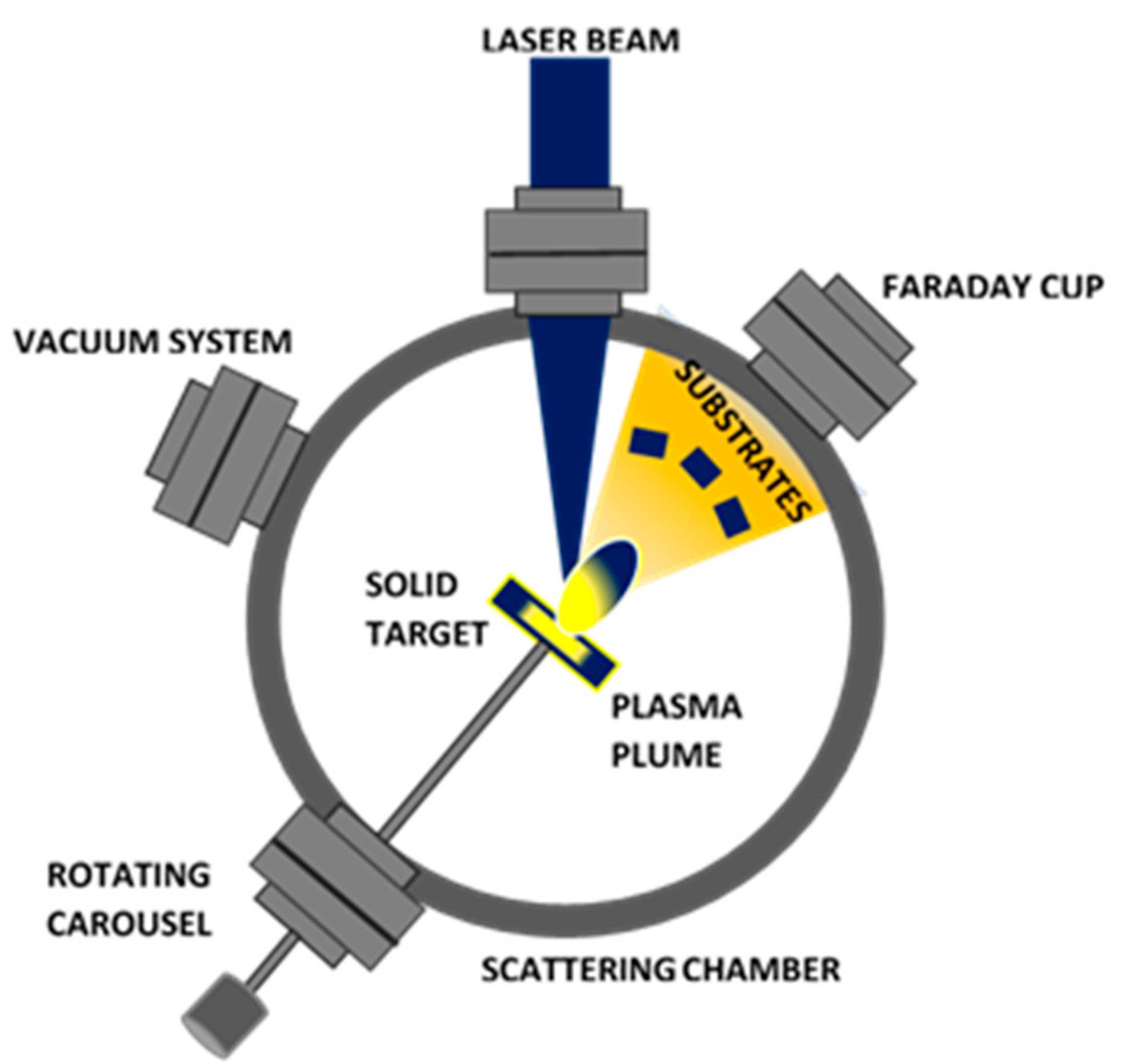
Pulsed laser deposition (PLD) consists of direct laser irradiation in a repetition rate mode of a solid target placed inside the scattering chamber in vacuum. The interaction induces local heating, vaporization, and ablation of the most superficial layers of the laser irradiated target. The formation of a plasma plume having a bright-colored appearance, which is a consequence of the ionization of the target, is generated at the ablation threshold of the material. The plume has a similar stoichiometry to that of the laser irradiated target material. The ions, atoms, and clusters, ejected during the laser-matter interaction, are deposited on the substrates placed in proximity of the solid target as reported in
Figure 1. PLD was performed at the laser energy of 100 mJ, at a 45° incidence angle from the target surface, with a focused laser beam spot on the solid target of 1 mm in diameter, in the repetition rate mode (1 Hz), through a quartz window, for 1 h. The laser fluence was about 12.6 J/cm
2. Substrates of PDMS were placed at ±15° with respect to the normal target surface and at 10 cm from the main target, as shown in
Figure 1. The energy of carbon ions generated during the interaction of the laser with the HOPG target was recorded in time of flight by a Faraday cup [
9] fixed at 30° and 1 m distance with respect to the normal target surface.
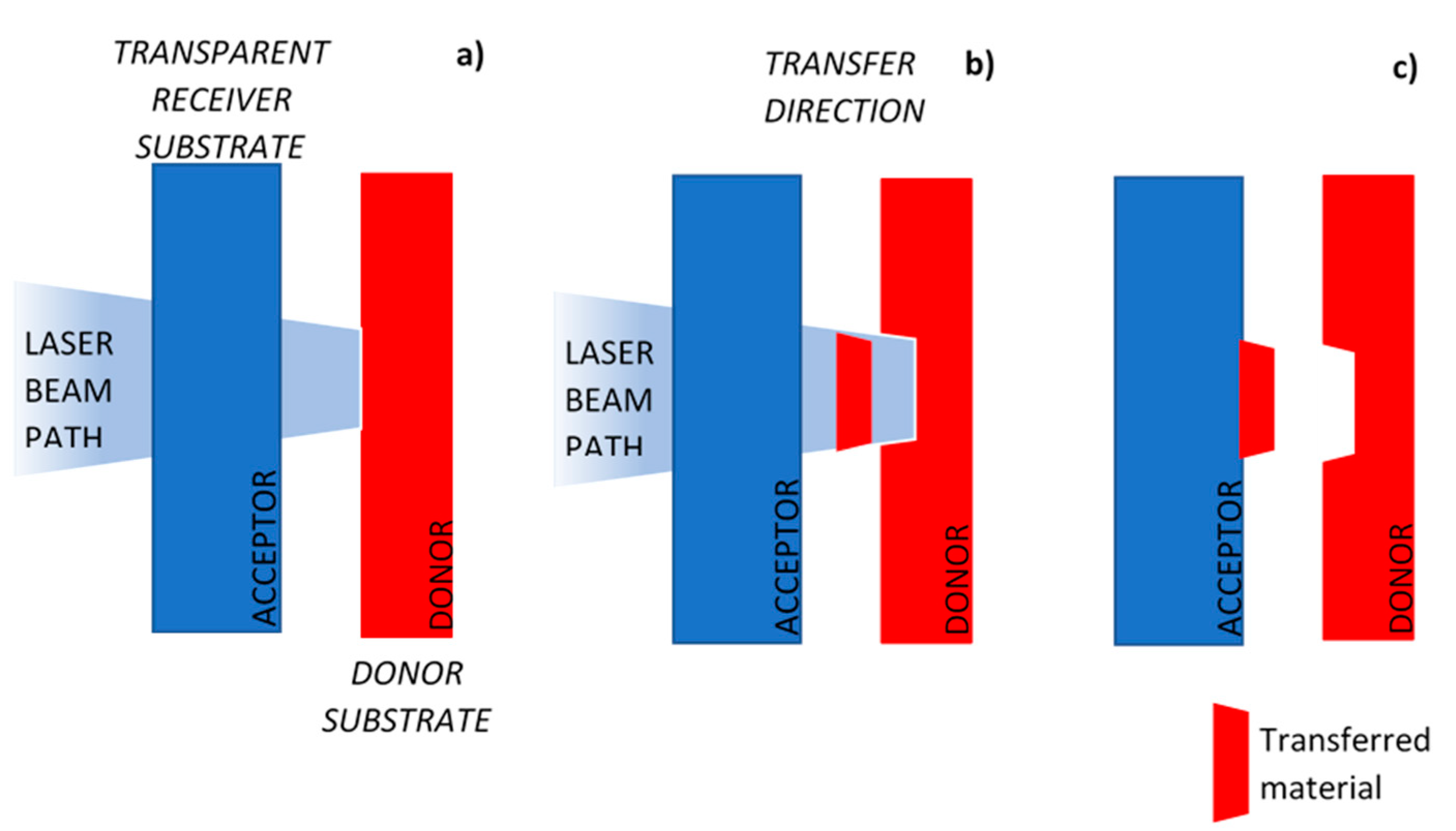
In the Laser-induced backward transfer (LIBT) process, a pulsed laser is used to induce the transfer of material from a main target (donor) on a substrate placed close or in contact with the source. The material transfer is in the opposite direction as the laser propagation [
10]. Typically, in air, the laser beam passes through the transparent substrate and hits the solid target (donor). At the laser energy threshold, which is higher than the ablation yield, material is ejected from the target and pushed toward the substrate (acceptor). The illustration of the processing is displayed in
Figure 2.
LIBT was performed at the laser energy of 375 mJ at a 0° incidence angle from the target surface, with a focused laser beam spot on the solid target of 1 mm in diameter and the laser operating in the repetition rate mode (2.5 Hz) for 5 min. The laser fluence was about 44.8 J/cm2. Substrates of polydimethylsiloxane were placed behind the target surface, parallel and at 10 mm from the main target. Both the acceptor and the donor were placed in a stage moved by x-y motors and controlled by a homemade software written in LabView, which proved to be versatile for different laser pulse durations and spot sizes. In our experiment, the laser scans an area of 8 mm × 8 mm along the row directions at a scan resolution of 1 mm and at a velocity of 2 mm/s.
2.1. Rutherford Back-Scattering (RBS) Spectrometry
The elemental composition of samples before and after the laser ablation processing was investigated by the RBS and ERDA (Elastic Recoil Detection Analysis) techniques using a beam of 2.6 MeV He
2+ ions at an incidence angle of 70°. At the scattering angle of 160°, a surface barrier silicon detector (Ortec, USA)) was placed to monitor the scattered alpha particles. The recoiled hydrogen atoms were collected at a scattering angle of 35° by a silicon detector with a 4 µm PP (polypropylene) filter to stop the forward scattered helium ions, the heavier nuclei and to transmit the energetic proton atoms. The ion current was maintained at 5.3 nA and the irradiation time at 500 s. The conversion from the energy scale to the concentration depth profile for RBS and ERDA was performed using the SIMNRA simulation code [
11].
2.2. Optical Measurements (UV-VIS)
The changes of the optical properties of the laser deposited PDMS substrates were studied by the UV-Vis spectroscopy using the AvaSpec-2048 spectrometer (Avantes, Apeldoom, Netherlands) equipped with an UB-600 lines/mm grating and operating from 195 nm to 757 nm. In our experiments, a dual source, formed by Halogen/deuterium lights, probes the wavelength range between 350 and 750 nm. One fiber optical connected to the source was placed at 0° in front of the sample, whereas a second fiber optical connected to the spectrometer was located behind the sample at −180° in the transmission mode.
2.3. Contact Angle Measurements
The changes of the hydrophobicity of the PDMS substrates deposited by the PLD and LIBT techniques were studied by the sessile drop technique. A distilled water drop in a volume of 3 µL was poured on the surface of the samples to measure the contact angle using the optical microscopy [
12]. The contact angle observed at the liquid/solid and at the liquid/air interfaces was measured in several different areas on the same sample from which an average standard deviation value was acquired.
2.4. Scanning Electron (SEM) and Atomic Force (AFM) Microscopies
The morphology, micro-structure, and roughness of the virgin and deposited samples were monitored by scanning electron (SEM) and atomic force microscopies (AFM). A LYRA3 GMU (Tescan, Brno, Czech Republic) in the secondary-electron mode at an acceleration voltage of 5 kV was employed for the SEM analysis on areas of 30 × 30 µm2, 3 × 3 µm2 and 1.5 × 1.5 µm2.
A Dimension ICON AFM (Bruker Corp., Billerica, MA, USA), operating in the ScanAsyst mode in air was used for determination. Silicon Tip on Nitride Lever (SCANASYST-AIR probe) with a spring constant of 0.4 N/m was employed for the AFM analysis on area of 1 × 1 µm2. The data processing was performed by the NanoScope Analysis software.
2.5. Tensile Stress Measurement
A mechanical tensile stress system was used to measure the strength of PDMS before and after deposition of HOPG by PLD and LIBT. A load ranging between 0.00981 and 0.981 N was used to measure the tensile force of virgin and modified materials. The analysis was performed at room temperature, repeating the measure three times from which the average measure was given.
3. Results
The multi-species and multi-energy streams of ions, generated during the interaction of the laser with the solid target, are ideal for implantation/deposition. Depending on their energy, they can reach different depths and induce structural, chemical, and physical modifications in the materials.
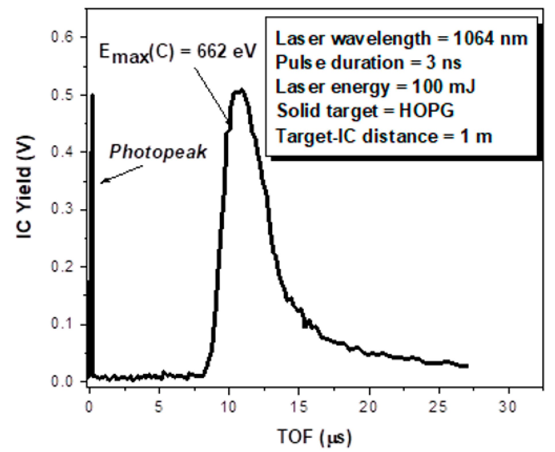
A Faraday cup (FC) detector was used to determine the energy of the emitted ions in the Time-Of-Flight (TOF) configuration [
9] during the PLD processing.
Figure 3 shows the FC spectrum achieved by a HOPG target at an energy of 100 mJ. The first sharp and very narrow peak is due to the photoelectric effect. The following broad peak corresponds to the convolution of signalar of fast protons, followed by contaminants such as C and O at a different velocity. In
Figure 3 the carbon ions are detected at 9.7 µs, indicating a maximum carbon energy of about 662 eV.
The produced C ions due to the low energy deposition during the PLD exhibit dominant nuclear stopping power responsible for the erosion rate, the surface rough-ness and the sputtering effects, on the surface of the deposited substrate.
The RBS analysis does not discriminate the carbon deposited on PDMS from the carbon contained in its bulk. In the next experiment, a layer of chemically different material from the bulk will be deposited on HOPG to mark the presence of carbon deposited on the PDMS substrate. However, considering previous our measurements at the same experimental and laser conditions (at the 12.6 J/cm2 fluence) herein described for PLD in vacuum, the ablation rate was about 0.6 µg/pulse, corresponding to a deposited thickness of about 20 nm. During LIBT in air, the fluence was about 45 J/cm2, inducing an ablation rate of about 2.7 µg/pulse and a deposited thickness of about 190 nm.
The average elemental composition in atomic percentage of the most superficial layer of the samples deposited by PLD and LIBT and evaluated by RBS and ERDA is reported in
Table 1.
The changes in the hydrogen, oxygen, and carbon concentration evaluated by RBS and ERDA analyses refer to the virgin PDMS and deposited PDMS + HOPG probed in a layer of about 500 nm. The carbon concentration increases of 68.1% by PLD and 42.2% by LIBT due to the presence of the thin carbon layer deposited on the PDMS matrix. In the case of PLD in vacuum, the deposition was performed in an environment in which hydrogen, oxygen, and other gases are desorbed from the matrix surface. In the case of LIBT in air, the deposition was performed in an environment rich in oxygen, carbon oxide, and water, i.e., in a condition favorable to the formation of carbon-hydrogen chemical bonds. We assume that the amount of hydrogen in the PLD sample is attributable to the hydrogen accumulation at the PDMS-HOPG interface and hydrogen absorption in the deposited carbon film. On the contrary, in the sample deposited by LIBT, the hydrogen content depends on the chemical bonds between the carbon radicals and the present hydrogen Due to humidity. The increase of oxygen after LIBT is imputable to the in air-processing. The increase of Si in LIBT could be due to the generation of silicon clusters and nanoparticles when, during the processing, the laser passes through PDMS, inducing the carbon ablation and Si nucleation in accordance with ref [
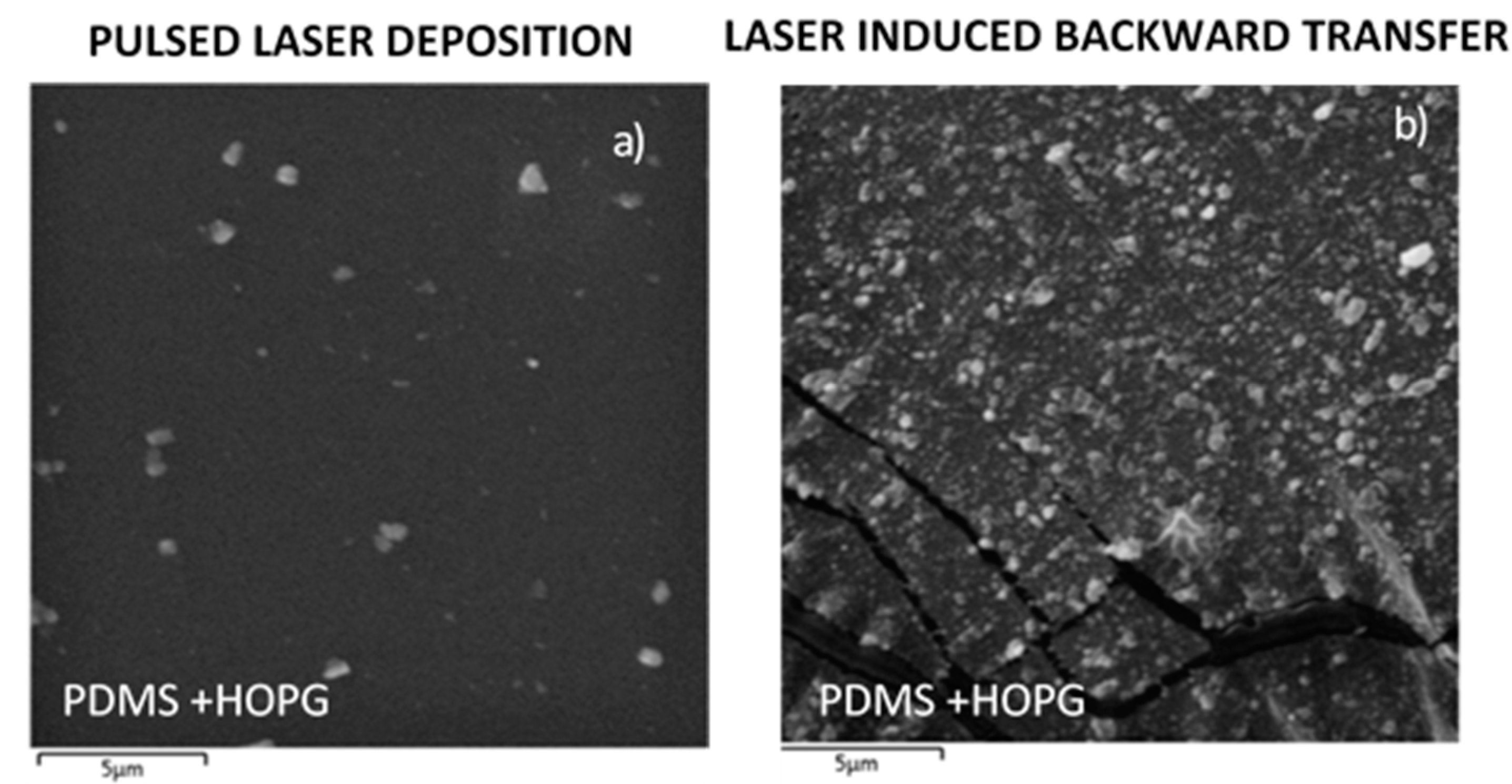
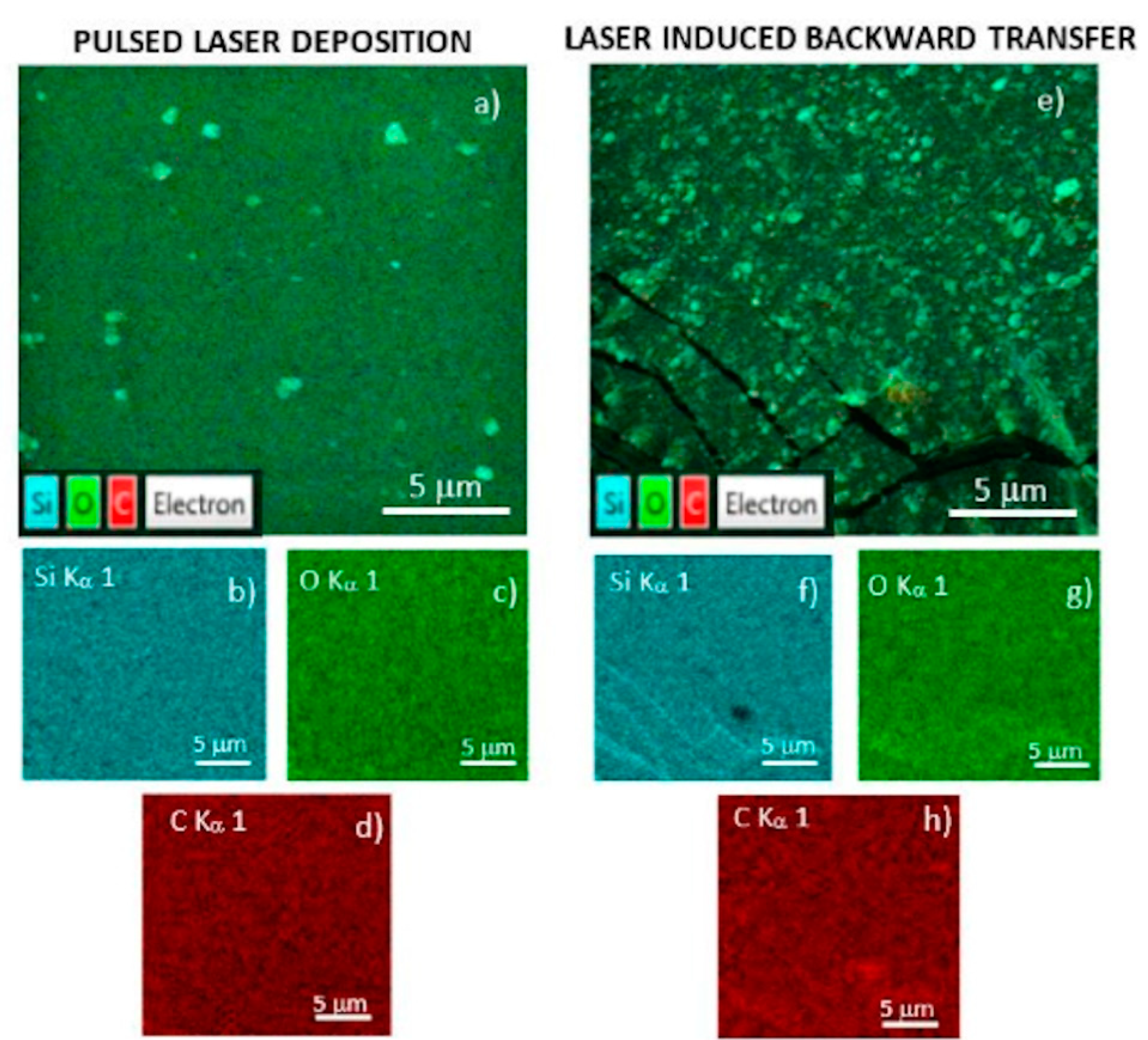
13]. Quite uniform layers of micron-sized grains are observed on the SEM images reported in
Figure 4.
Figure 4 remarks the difference in the deposited coating, which appears poor but without cracks in PDMS deposited by PLD and rich with fractures and rifts on the surface when LIBT is employed.
Figure 5 displays maps obtained considering the C, O, and Si Kα lines given by the energy dispersive x-ray spectroscopy (EDX) coupled to SEM. The red regions covering the images confirm that C homogeneously covers the silicon-based structures on the PDMS matrix. The big size particles, appearing in small concentration on PDMS deposited by PLD and in high concentration on PDMS treated by LIBT, are clusters of silicon-based material enfolded with C in agreement with the optical absorption analysis and are ascribable to the laser-matter interaction [
13].
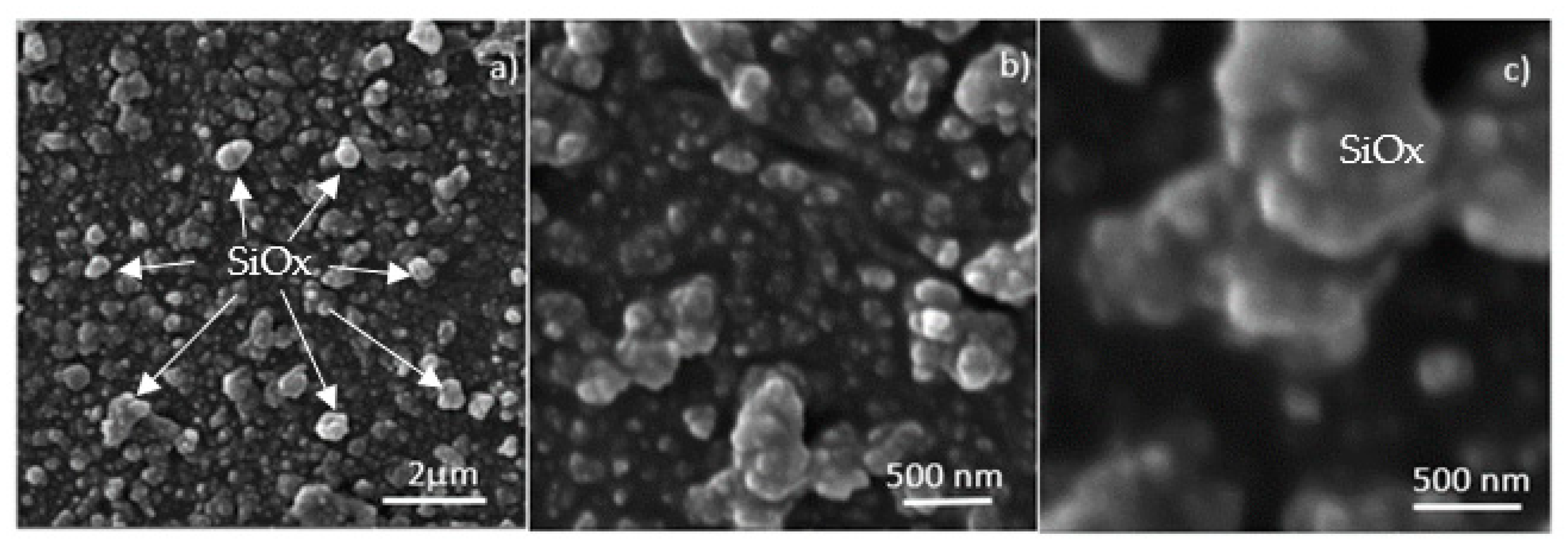
In
Figure 6, SEM images are reported with magnification of 20.8 k×, 69.2 k×, and 208 k× of PDMS matrices deposited by LIBT with HOPG. The nano-scaled structures, with dimensions in the range of 20–100 nm on PDMS with HOPG, are visible in
Figure 5c. The observed nanoparticle dimensions are comparable with the values reported in the literature for deposition in RT conditions [
14].
Figure 6 shows, in addition to a nanometer-sized distribution of C structures, nanostructures of Si and Oxygen with a stoichiometry compatible with SiO
2 in agreement with
Table 2, which displays the atomic percentage concentration of the individual elements of the coating layer deposited on the surface of PDMS by the PLD and LIBT techniques. Some of the more significative SiO
x structures are pointed out by arrows. The EDX analysis was performed on five samples in different areas, and the results within the 10% error are presented in
Table 2.
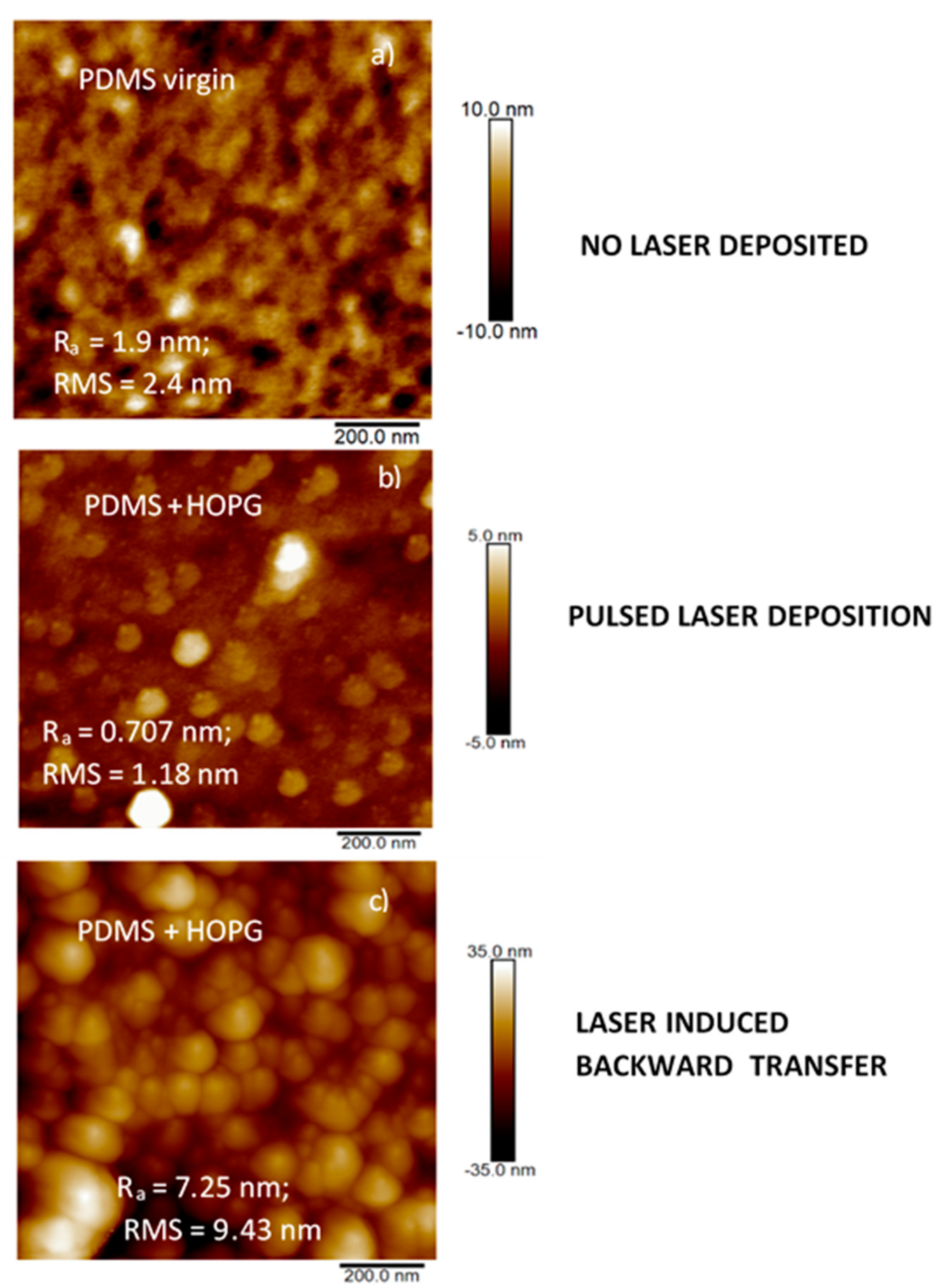
Figure 7 reports the roughness together with the size of structures hosted in the composites and generated by the PLD and LIBT processing, which were measured by AFM.
The difference between the surface (basic) of the investigated area and the rough surface (real) in the investigated area increased from 1.10% in HOPG deposited on PDMS by PLD to 6.75% in HOPG deposited on PDMS by LIBT, respectively. This trend points out an increase in roughness in agreement with the reported RMS (Root Mean Square) roughness values of 1.18 nm and 9.43 nm, respectively.
The size of the structures deposited on the surfaces of PDMS by PLD lower than 1 µm is ascribed to the low energy of deposited ions during the PLD processing. The size of the structures generated by LIBT of about 13.9 nm is maybe due to the thermal effect induced by the highest plasma temperature.
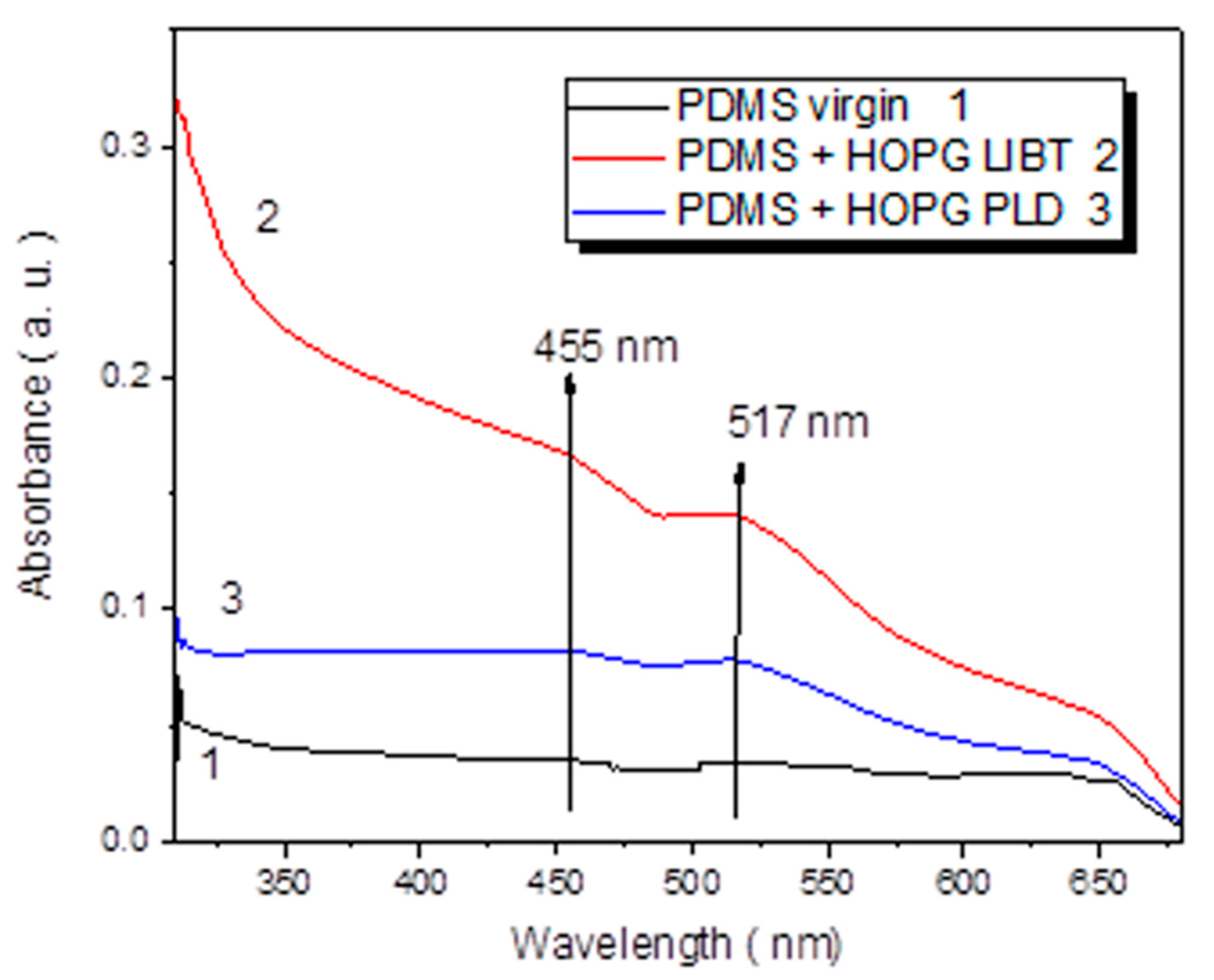
The optical measurement of PDMS deposited with HOPG by LIBT, whose spectrum is shown in
Figure 8 (curve 2), reveals a steep rise in absorbance, particularly in the near UV region. This can be ascribed to the compositional changes in the polymers: the concentration and the size of the deposited oxides and carbon structures. Samples deposited by LIBT, in addition to showing the highest absorbance, are characterized by absorption bands around 455 nm and 517 nm. These last two absorbance bands are identifiable also in PDMS deposited by PLD (curve 3 in
Figure 8). In this latter case, the lowest intensity is ascribable to the low concentration of deposited material in accordance with the SEM and AFM analyses. The steep rise in absorption in the near UV wavelength region is likely to be due to formation of unsaturated groups and presence of carbonyl and hydroxyl groups in the polymer due to the laser irradiation in air. The main effects of laser irradiation are chain scissions and crosslinking, accompanied by the formation of unsaturated products in the polymer chain. Free radicals produced in the polymer by the laser radiation can react with oxygen in air and form such groups [
15].
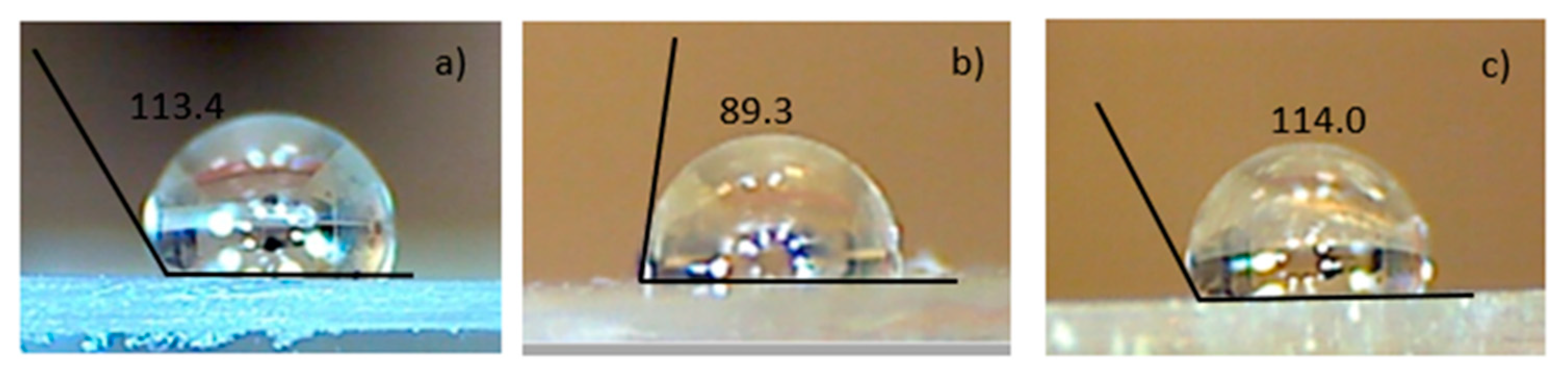
The contact angle formed when a drop of distilled water was poured on the samples, which was measured before and after the laser treatment, as reported in
Figure 9.
The high contact angle indicates that the liquid does not spread well on the surface while the low contact angle displays high spreading. If the contact angle is greater than 90°, as for virgin PDMS, the surface is said to be hydrophobic, indicating non-wetting with that liquid. The contact angle for virgin PDMS is 113.4°. After the laser deposition of HOPG and by PLD, the contact angle decreases to 89.3°, while it increases to 114.0° after the deposition of HOPG by LIBT.
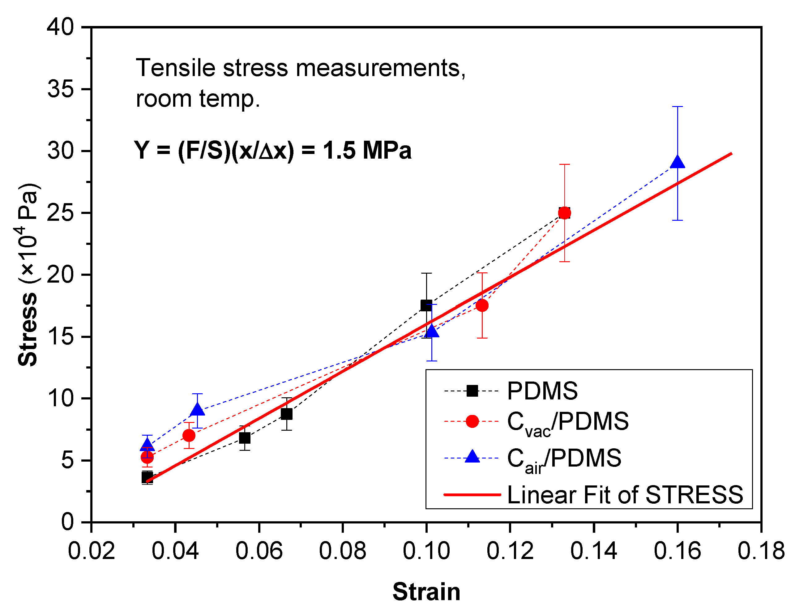
Figure 10 shows the tensile stress analysis to evaluate the elasticity changes in the PDMS substrates after the PLD and LIBT processing.
The average Young’s modulus was obtained using different loads for 10 s, and repeating the measure 3 times, which resulted in about 1.5 MPa for virgin PDMS and deposited PDMS both in vacuum and in air. The obtained measures are affected by an error of 15%. No significant changes of the Young’s modulus have been revealed in all samples, likely due to the small thickness of the deposited material compared to the bulk thickness. The Young’s modulus is about 1.5 MPa at room temperature. This value is comparable with the ones reported in literature [
16].
4. Discussion
During the ablation of material from a solid target by laser, the transition from the thermal ablation to the explosive boiling (i.e., the phase explosion) takes place depending on the rapid target heating. This effect is a function of the laser fluence and wavelength. The threshold at which the phase explosion is expected to occur is between 30 J/cm
2 and 55 J/cm
2, as reported in literature [
17]. The laser fluence adopted in PLD is lower than the mentioned threshold; indeed, the production of large particulates and broad clusters as a consequence of the phase explosion is not significant, raising the quality of the deposited film. On the contrary, the laser fluence in LIBT of about 44.8 J/cm
2 justifies the amount and the size of the large structures formed on the surface of the matrix as reported by SEM, EDX, and AFM images. The decrease of the hydrogen amount and the increase of carbon contents reported in
Table 1 indicates changes in the physical properties of PDMS after the pulsed laser deposition. In the film deposited on the substrate by PLD, hydrogen is accumulated behind and inside the coating while in that obtained by LIBT, hydrogen is absorbed by a thicker carbon coating layer and encapsulated during the film growth in air.
The surface of substrates deposited by PLD and LIBT shows spherical structures. The more pronounced increase in the surface roughness, observed on PDMS deposited with HOPG by LIBT, is likely due to the transition from thermal ablation to the phase explosion that occurs during LIBT processing.
The absorption bands at 455 nm corresponding to 2.725 eV and 517 nm corresponding to 2.407 eV can be due to the Si-based nanostructures coated with carbon [
18]. The steep rise in absorbance in the samples deposited by LIBT is consistent with the presence of opaque nanostructures with an average size distribution around (20–100) nm, as confirmed by the SEM analysis.
It is well-known that the contact angle is correlated with the surface roughness, the heterogeneity, the particle shape, the particle size, the crystalline structure, and the chemical compositions of the films formed on the surfaces of the substrates. The roughness dependence of wettability has different trends in different roughness ranges [
19]. It seems that PLD processing induces slight turning from hydrophobicity to hydrophilicity while LIBT induces an improvement of the hydrophobicity. The values deduced for virgin PDMS and PDMS+LBIT are higher than the one obtained after the PLD processing.
For the values reported by AFM, it seems that lowering (or increasing) the surface roughness induces the decreasing (or increasing) of the contact angle and consequently, indicates higher (or lesser) wettability. The contact angle analysis in agreement with AFM indicates that the highest sized structures produced during the LIBT processing affect the wettability, which is a crucial value for biomedical applications and the manufacturing technology.
5. Conclusions
In the present study, the comparison between the deposited films obtained by PLD in vacuum and LIBT in air has been investigated. The laser-ablation mechanism varies in the different environments.
The laser-matter interaction in vacuum produces plasma at the surface of the target material, which expands considerably in the vacuum chamber. In vacuum, the debris materials from the expanding plume have different speeds. Typically, in vacuum, the nanoparticles are directly generated from the target material by ejection of material removed from its surface. The ablation rate is higher in vacuum than in air [
20].
The ablation threshold in air is 50% lower than that in vacuum because, due to the air resistance, the hot plasma expands at a slower speed than in vacuum, accelerating the ablation effect. In air, higher thermal damage has been observed than in vacuum since the ejected material can propagate away from the target material with a low resistance within the shock waves. Moreover, the plasma produced in air by LIBT was found to be much hotter and denser than that produced in vacuum [
21], causing more mechanical degradation than PLD. Micro-cracks, breaking of the main chains of the macromolecule, emission of low molecular weight gaseous products, and oxidation of the polymer can occur. The thermal and explosive effects observed at the different experimental and laser conditions result in the production of clusters and particulates small in size and in quantity in the case of PLD and large in size and high in number in LIBT, affecting the quality of the deposited film.
The type, energy, and dose of the deposited ions as well as the matrix features are crucial for both the effective changes of the compositional, optical, and surface properties and to facilitate different functionalities, such as the cell proliferation, tissue growth, repair, and antimicrobial agents.
The X-ray microprobe of SEM-EDS confirmed the presence of nanocrystal of SiO2, which led to both the enhancement of wettability under PLD in vacuum and increase of the hydrophobicity under LIBT in air. These results are interesting considering how much the wettability can affect the biological performances and the detection of cellular responses. PLD in vacuum avoids contamination during the processing and allows to obtain good stoichiometry on the deposited films in comparison to the deposited films obtained by other physical chemical deposition techniques, such as electrophoresis and ion sputtering. The so-obtained films contain a very low amount of oxidizing impurities and are strongly adherent to the substrate. On the other hand, LIBT is a more simple and versatile process allowing for good spatial control of the deposition of complex materials for patterning, but it occurs in air, therefore promoting oxidation and nitridation effects.
Elasticity and wettability are critical features for depositing films for joint implants and biosensor. The wettability of PDMS deposited by PLD improves due to the more uniform coating formed by small size nanoparticles. The stress-strain curves analysis indicates that the samples modified by both techniques do not exhibit notable changes due to the small deposited thickness related to the bulk one.
Further optimization of the LIBT process will include: (i) optimizing the condition for the precise patterning on different type of substrates; (ii) inducing localized transfer in smaller areas; and (iii) improving the quality of the transferred material for the fabrication of devices based on 2D materials (graphene, molybdenum disulphide, phosphorene). The improvement of LIBT is also promising to eliminate several time-consuming lithographic processing steps and at the same time to allow good quality patterns without the use of masks in the localized selected areas on the device.


 ,
, 


