Article

Characterisation of Channel Waveguides Fabricated in an Er3+-Doped Tellurite Glass Using Two Ion Beam Techniques

1
Wigner Research Centre for Physics, P.O. Box 49, H-1525 Budapest, Hungary
2
Atomki, Institute for Nuclear Research, P.O. Box 51, H-4001 Debrecen, Hungary
3
Centre for Energy Research, Konkoly-Thege Rd. 29–33, H-1121 Budapest, Hungary
4
Nuclear Physics Institute AV CR, 250 68 Řež near Prague, Czech Republic
5
Istitute of Microelectronics and Technology, Óbuda University, P.O. Box 112, H-1431 Budapest, Hungary
*
Authors to whom correspondence should be addressed.
Chemosensors 2022, 10(8), 337; https://doi.org/10.3390/chemosensors10080337
Submission received: 11 June 2022 / Revised: 8 August 2022 / Accepted: 15 August 2022 / Published: 17 August 2022
(This article belongs to the Special Issue Optical Chemical Sensors and Spectroscopy)

Abstract

:
Two methods were proposed and implemented for the fabrication of channel waveguides in an Er-doped Tellurite glass. In the first method, channel waveguides were fabricated by implanting 1.5 MeV and 3.5 MeV energy N+ ions through a special silicon mask to the glass sample at various fluences. Those waveguides implanted at a fluence of 1.0 × 10¹⁶ ions/cm2 operated up to 980 nm, and showed green upconversion of the Erbium ions. In the second method, channel waveguides were directly written in the Er3+: TeO2W2O3 glass using an 11 MeV C4+ ion microbeam with fluences in the range of 1 · 1014–5 · 1016 ions/cm2. The waveguides worked in single mode regime up to the 1540 nm telecom wavelength. Propagation losses were reduced from the 14 dB/cm of the as-irradiated waveguides by stepwise thermal annealing to 1.5 dB/cm at λ = 1400 nm.

1. Introduction

Photonics technology is part of virtually every branch of modern industry, healthcare and everyday life. One of its first and most important applications is in telecommunications. Photonics has found its more recent applications in precision instrumentation, defence, healthcare, sensing, automotive industry and aerospace. The introduction of photonic integration in optics in the last 20 years was a revolutionary change, similar to that caused by the invention of integrated circuits in electronics 60 years ago.
The evolution of the optical industry for a long time consisted of the improvement of the basic components, finding the best materials and developing better techniques for device fabrication. Photonic technology has largely been standardised by now. Standard technologies are used in the fabrication of optical chips.
Electronic chip features are now in the order of ten nanometres. The rapid decrease of feature size has rendered older microelectronic fabrication facilities obsolete. Since the feature size of photonic components is in the order of a few hundred nanometres, photonic companies are using modified “old” microelectronic facilities to fabricate photonic chips.
The fabrication of optical integrated circuits, just as that of their electronic counterparts, involves a number of successive steps.
Integrated optical and optoelectronic devices have two basic components: waveguides and gratings [1,2]. In-diffusion of metal ions [3], ion exchange [4,5], sol-gel techniques [6], ion beam implantations/irradiation [7], epitaxial layer deposition by sputtering [8], molecular beam epitaxy [9], pulsed laser deposition [10] and chemical vapour deposition [11] are used for waveguide fabrication in optical materials
Ion beam implantation is an outstanding technique for waveguide fabrication, thanks to its applicability to a wide range of materials, and the very good controllability of the dimensions and refractive index profile of the waveguides [12,13,14,15,16,17,18]. Ion-beam-implanted optical waveguides usually either maintain the optical properties, such as the optical luminescence spectra, of the non-implanted bulk or regain them after an adequate thermal annealing.
Since the first documented application of ion beam implantation to waveguide fabrication in 1968 [19], waveguides in over a hundred optical materials have been produced using this technique. The energies of the implanted ions were typically between a few hundred keV and several MeV [20,21,22,23].
However, in spite of the extensive research work carried out since the first publication in this field, about 50 years ago, ion beam implantation is still far from being a well-established technology. The main drawback of using ion beam techniques for the fabrication of integrated optical elements–besides of the need of access to a low-energy particle accelerator–was the fact that fluences in the order of 1015–1017 ions/cm2 needed to be applied to the sample to cause a refractive index change adequate for the fabrication of a low propagation loss optical waveguide. This holds true especially when the mass and energy of the implanting ion are low (e.g., hydrogen or helium ions of energies up to a few MeV). The use of the so-called swift heavy ions (SHI) about 15 years ago dramatically reduced the required fluences necessary to produce integrated optical elements down to 1011–1013 ions/cm2, consequently reducing the fabrication time for an element at a given ion current density. This is due to the fact that, in those cases, electronic interaction among the implanted ions and the atoms in the sample becomes dominant over nuclear interaction, the latter being more important at lower ion mass and energy. The first studies on the effects of swift heavy ion irradiation on the optical properties of materials date back to the 1990s [24].
As for the implanted ions, in the first two decades, mainly light and medium mass ions of moderate energy (up to about 5 MeV) were used, due to the limitations of the available one-stage Van de Graaff accelerators. The development of the TandetronTM (HVE) accelerators made it possible to use swift medium mass and heavy ions for the fabrication of optical waveguides.
Depending on the target material (optical crystal or glass) and the implanted ion, refractive index changes were produced mainly either by electronic or nuclear interaction [25,26,27,28,29].
The simplest method to produce channel waveguides is via the use of masks to allow implantation only in the open areas, while ions stop in the mask layer before reaching the target surface. The development of ion microbeam-forming devices made it possible to write the channel waveguides directly.
An example of the first method is the work of Vazquez et al. [30]. They produced channel waveguides in a soda lime (Er3+/Yb3+)-doped glass. As the greatest part of the researchers in this field, they measured propagation losses of their waveguides only at visible wavelengths.
As for the early research work on direct microbeam writing of channel waveguides, the greatest part of them used proton microbeams [31,32,33,34,35].
Microbeam techniques significantly improve the flexibility of the fabrication of components.
An example of proton-beam-written channel waveguides is the work of Roberts and von Bibra [31]. Their buried waveguides had a very low propagation loss of 0.5 dB/cm at 632.8 nm.
Bettiol et al. obtained propagation losses of 8.3 dB/cm at 632.8 nm in 2 MeV proton-microbeam-written channel waveguides in Foturan glass [32]. They also fabricated erbium-doped waveguide amplifiers (EDWAs) in an Er3+/Yb3+ co-doped IOG laser glass material [33]. They obtained low propagation losses (0.8 dB/cm at 1310 nm) and high gain (1.72 dB/cm) in the C telecom band, with a pump beam of 975 nm, after an additional thermal annealing.
Channel waveguide fabrication by proton beam implantation in chalcogenide glasses was reported by An et al. [34]. They achieved 2 dB/cm propagation losses at 1064 nm.
Direct proton beam writing at 1 MeV energy in Nd: YAG laser crystal was reported by Yao et al., with 4 dB/cm propagation loss in the channel waveguide [35].
As for the fabrication of channel waveguides and other two-dimensional integrated optical elements, the development of ion microbeam facilities attached to accelerators, proton and helium microbeams have been extensively used for producing optical channel waveguides and gratings, as well as other microoptical elements in organic and inorganic optical materials [27,35].
However, these “traditional” ion microbeam techniques still have not developed into a reliable routine technology.
It must be noted that this technique (often called proton beam writing or PBW) is not to be confused with FIB technology. In the case of FIB equipment, very low energy (1–50 keV) ions, usually coming from liquid metal ion sources (LMIS), especially gallium ion sources, are used. FIB is a well-established technology in the semiconductor industry, mainly used to defect analysis, circuit modification, photomask repair, imaging and micro machining. FIB is completely out of the scope of this project.
Our early research in the second half of the 1990s resulted in high-spatial frequency ion-implanted transmission optical gratings of acceptable diffraction efficiency, using standard photoresist masks, and implantation with N ions in the 500–1500 keV energy range [36].
More recently, in the framework of two successive Hungarian research projects (with international co-operation) we have fabricated planar optical waveguides in various optical materials, such as sillenite and eulytine type bismuth germanate (BGO), CaF2, rare-earth ion-doped and undoped LiNbO3 and Er: TeO2-W2O3 glass, using various light- and medium-mass ions of 1–5 MeV energy. The waveguides proved to be functional at the telecom C band (1550 nm) [37]. We adapted the method of multi-energy ion beam implantation for the use of higher energy medium mass ions, to allow for an improved control of the depth profile of refractive index in the planar waveguides, and hence increasing confinement of the guided wave. We succeeded in fabricating channel waveguides in an Er: TeO2-W2O3 glass, using 1.5 MeV N+ implantation through masks. Functionality and green upconversion at 980 nm were demonstrated [38]. This method is illustrated in Figure 1.
We also present our results in direct ion microbeam writing of channel waveguides in an Er-doped tungsten tellurite glass, using medium mass high-energy ions. Additional stepwise thermal annealing was also applied to the implanted sample. The channel waveguides underwent thorough structural and functional tests.
The main advantage of this method compared to previous methods is the significantly reduced fabrication time enabled by reducing the necessary fluence values to achieve high refractive index modulation.
These channel waveguides proved to be of single mode at the C telecom band. After the thermal annealing, their propagation losses were equal to or lower than of those fabricated by MeV energy focussed proton or He ion beam writing. Besides, of the fabrication of simple channel waveguides, we succeeded in producing more complicated structures, as well. Those results are to be published elsewhere soon.

2. Waveguide Design and Fabrication

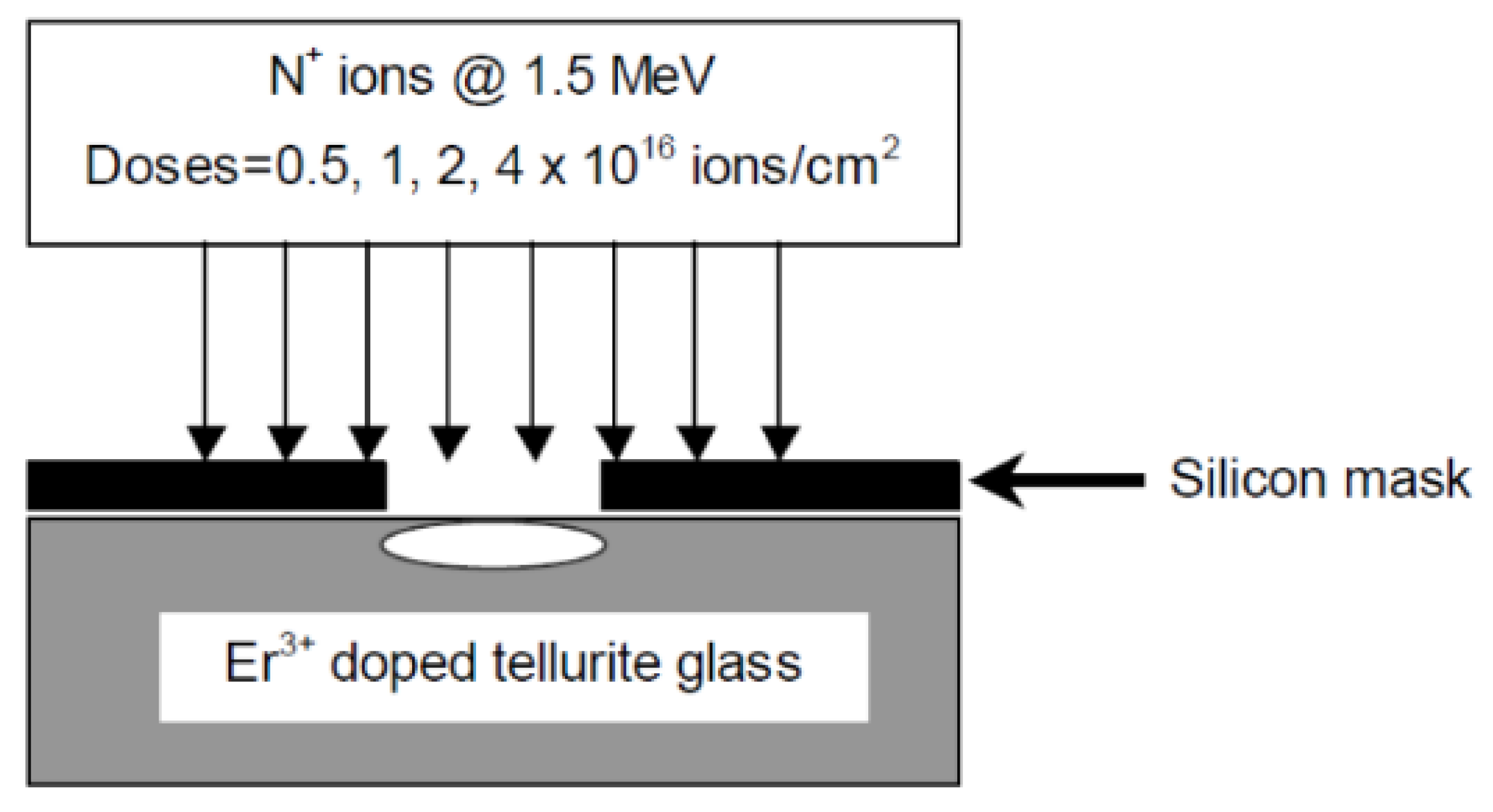
2.1. First Method: Implantation through a Silicon Mask

Channel waveguides were fabricated using the 5 MV Van de Graaff accelerator of the Wigner Research Centre for Physics (former Research Institute for Particle and Nuclear Physics) of Budapest. Implantation was carried out through a silicon membrane mask with 25 μm wide slits, with 1.5 MeV energy (E) N+ ions (as shown in Figure 1), and later with 3.5 MeV energy N ions, using difference fluences (F), namely 0.5, 1, 2 and 4 · 1016 ions/cm2.

2.2. Second Method: Direct Writing by an 11 MeV Carbon Ion Microbeam

Fabrication of the channel waveguides was carried out at the 3 MV Tandetron 4130 MC of the Nuclear Physics Institute AV CR, Řež, Czech Republic. Channel waveguides were directly written in the sample with a microbeam of 11 MeV C4+ ions.
Microbeam size for the channel waveguides in was 8 µm × 12 µm, the shorter size side of the rectangle being the width of the channel waveguides. The length of the channel waveguides was 9 mm. Irradiated fluences ranged from 1 · 1014 to 5 · 1016 ions/cm2. When irradiating a sample with medium- or heavier weight ions of high energies (Swift Heavy Ions) the predominant interaction with the target becomes the electronic one, instead of the nuclear one.

3. SRIM Simulation to Predict Waveguide Structure

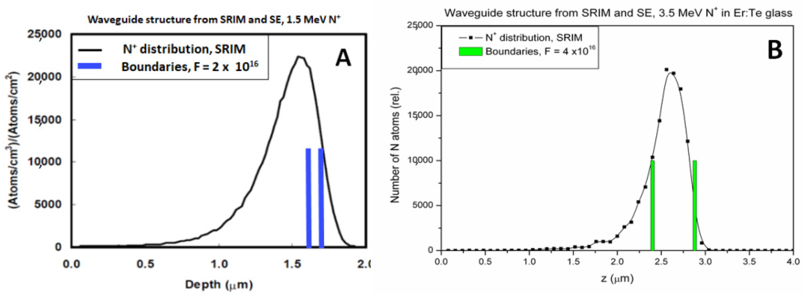
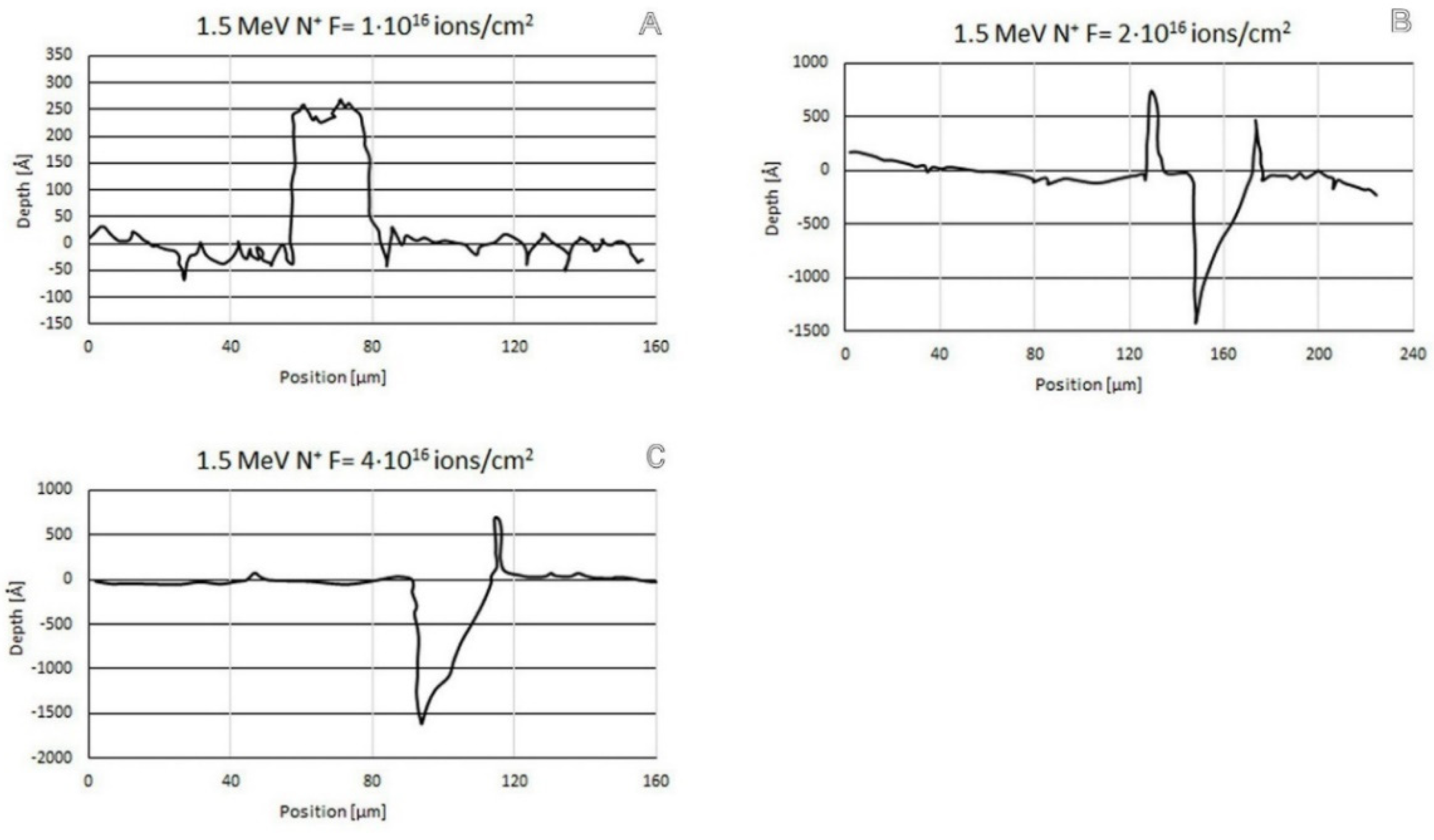
3.1. Implantation through a Silicon Mask

The depth of the waveguides was defined by the depth distribution of the implanted nitrogen and carbon ions in the glass sample. It was calculated with the Stopping and Range of Ions in Matters (SRIM) code [39]. The results for E = 1.5 MeV nitrogen ions are presented in Figure 2A. N+ ions penetrate down to around 2 μm below the surface, and the maximum of the distribution is at 1.5 μm. The depth structure of the waveguide (distribution of the index of refraction) has been calculated from the results of spectroscopic ellipsometry measurements performed on a planar waveguide implanted with the same 1.5 MeV energy N+ ion beam at the same fluence. The two blue bars in the figure represent the boundaries of the barrier layer. The thickness of the well of that waveguide was 1.6 µm, and that of the barrier was about 0.1 µm. Details of the spectroscopic ellipsometry experiments are presented in Section 6.
Another series of channel waveguides was fabricated by the above method, but using N+ ions of 3.5 MeV energy. Due to the higher longitudinal range of the 3.5 MeV N+ ions, those channel waveguides had deeper wells and wider barriers. This is demonstrated in Figure 2B. The calculated distribution of the implanted N+ ions (black line in Figure 2B) is centred at 2.6 µm below the sample surface. The depth structure of the waveguide has been calculated from the results of spectroscopic ellipsometry measurements performed on a planar waveguide implanted with the same 3.5 MeV energy N+ ion beam at the same fluence. The two green bars in the figure represent the boundaries of the barrier layer. The thickness of the well of that waveguide was 2.4 µm, and that of the barrier was about 0.4 µm.

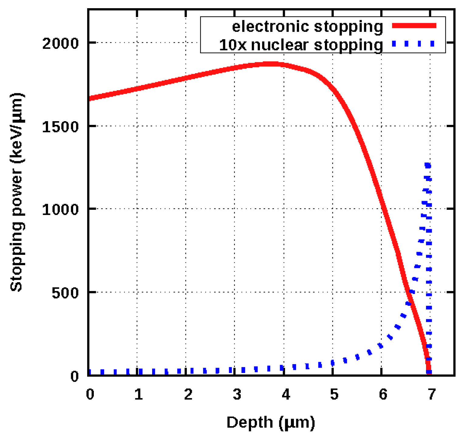
3.2. Direct Writing by an 11 MeV Carbon Ion Microbeam

According to the SRIM simulations, the maximum of the energy loss due to electronic interaction was at 3.8 µm below the surface, and that due to the nuclear interaction was at 6.9 µm, as can be seen in Figure 3. The maximum electronic energy loss was about 14 times higher than the nuclear one. Although the range of the 11 MeV C4+ ions is much longer than that of the 1.5 MeV and 3.5 MeV N+ ions, the thickness of the well of the planar waveguide in the first case will be determined by the amorphised barrier layer that will be created around the maximum of the energy loss. Thus, depending on the implanted fluence, the well thickness will be between about 3.5 and 0 µm. (The latter refers to a fully amorphised layer extending from the maximum of the electronic energy loss up to the sample surface.)

4. Microscopic Measurements of the Ion-Beam-Implanted Channel Waveguides

Microscopic study of the ion-beam-implanted channel waveguides made it possible to check their quality. Since polarisation and interference phase contrast microscopy were used, variations in the optical path across the channel waveguides could also be qualitatively assessed.

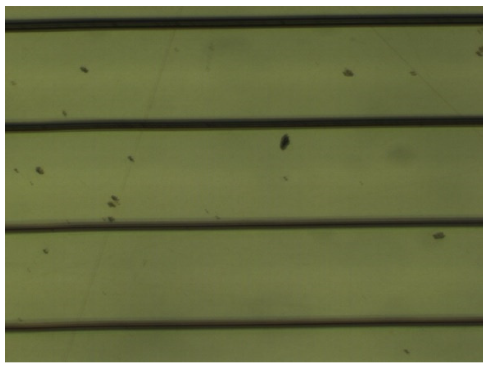
4.1. Implantation through a Silicon Mask

The implanted channel waveguides were examined using a Nikon reflection polarisation microscope. Optical path variations were transformed into hue variations of interference colours. Microscopic images of all channel waveguides implanted at all the fluences are presented in Figure 4. One can see that higher implanted fluences created larger optical path modifications in the channel waveguides. It must be noted that this kind of microscopy, when using only dry objectives, shows the total optical path variation, including changes in both the refractive index and the surface height. To separately measure the two effects, either the use of an immersion objective with an immersion oil with refractive index well matched to that of the implanted channel waveguide, or surface profilometry are needed.

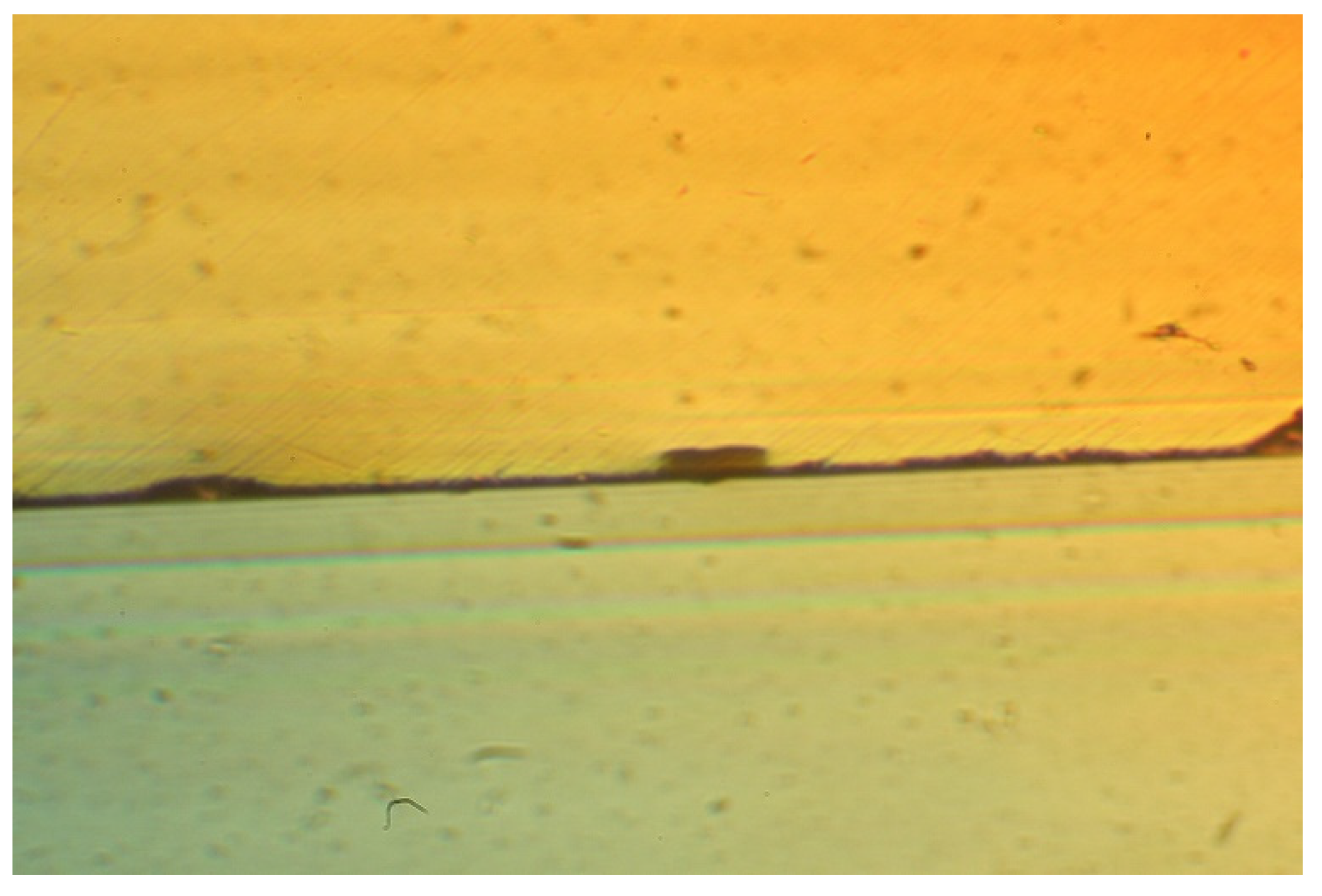
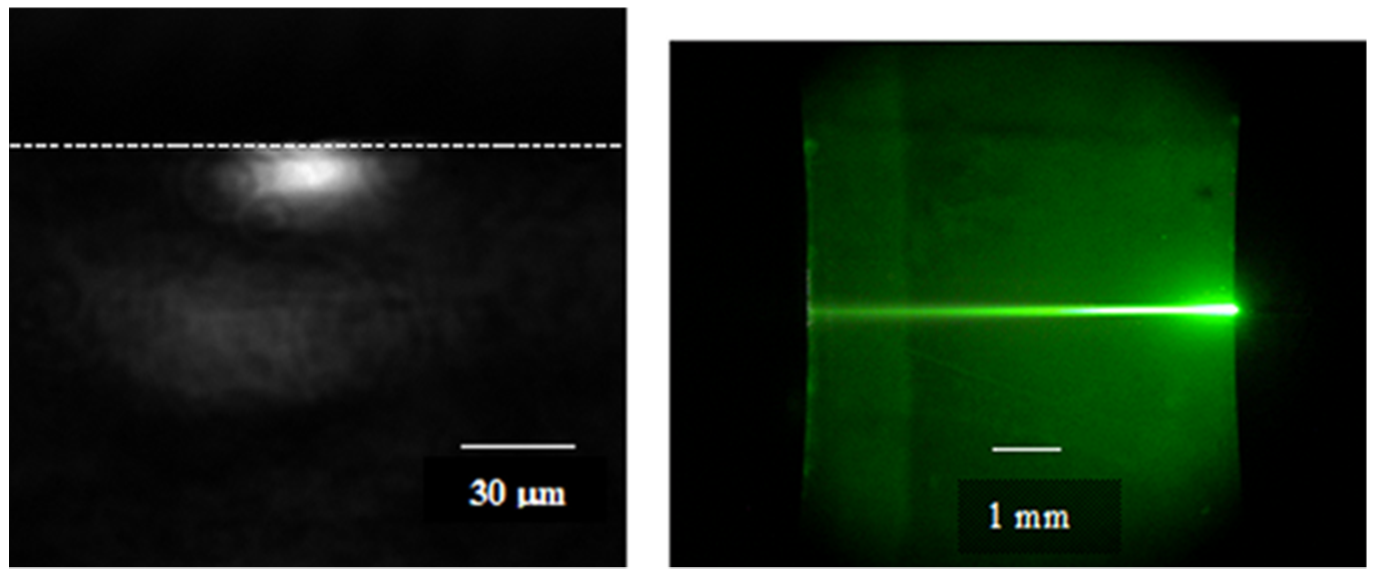
4.2. Direct Writing by an 11 MeV Carbon Ion Microbeam

The 11 MeV carbon-microbeam-implanted channel waveguides were also examined using the same Nikon reflexion polarisation microscope. Four channel waveguides can be seen in Figure 5. Implanted fluence decreases from top to bottom.
The same sample was also studied by an interference phase contrast (INTERPAHKO) microscope. A microphoto with details of four channel waveguides can be seen in Figure 6.
It was found that performing transmission INTERPHAKO microscopy on the well-polished edge of the sample could yield very clear and well-defined images of the end faces of the implanted channel waveguides. An example is shown in Figure 7. The width of the channel waveguide was 15 µm and its depth was about 3.3 µm.

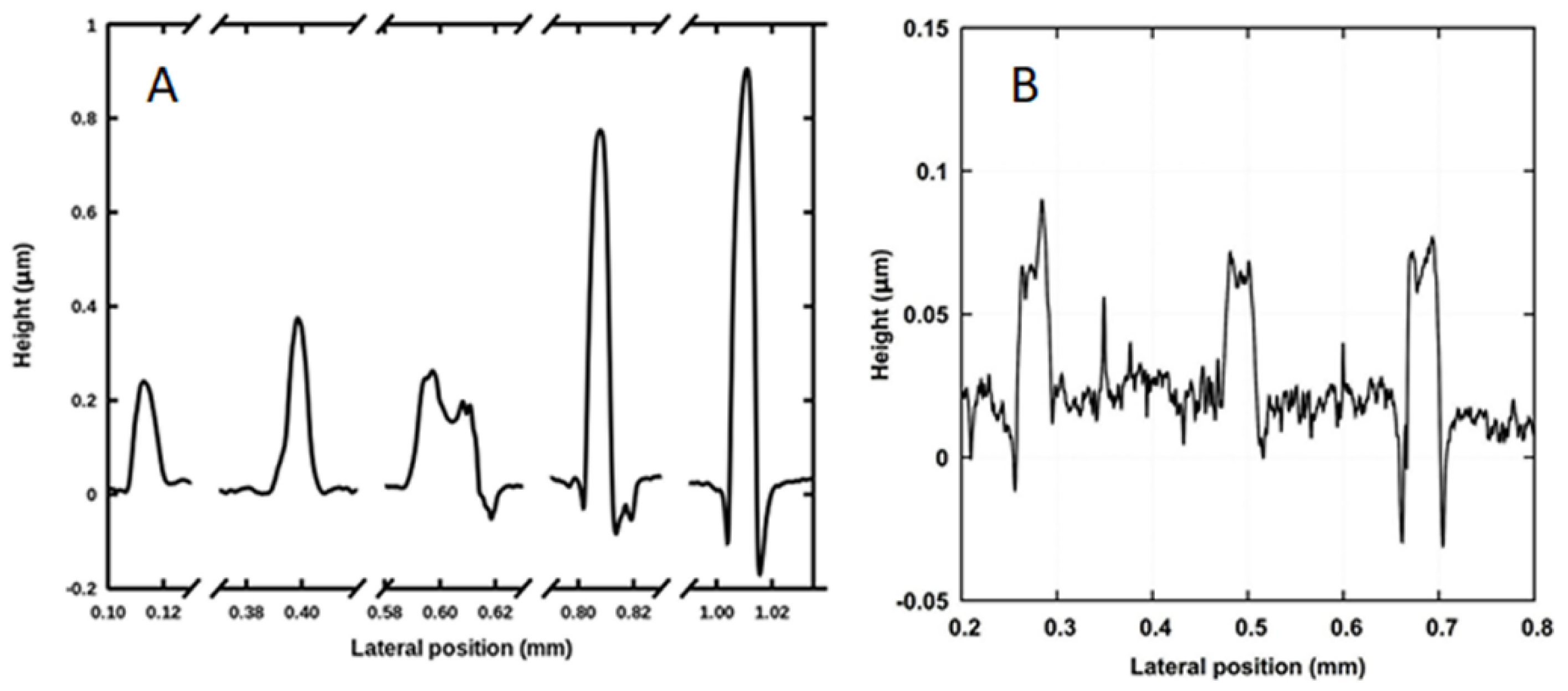
5. Measurements of the Surface Profiles of the Ion-Beam-Implanted Channel Waveguides

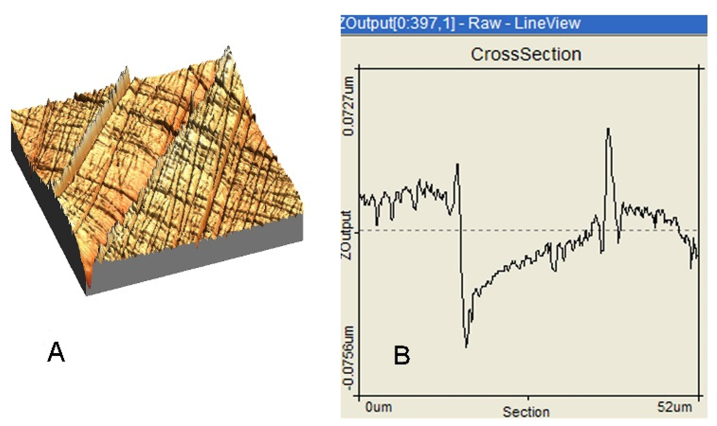
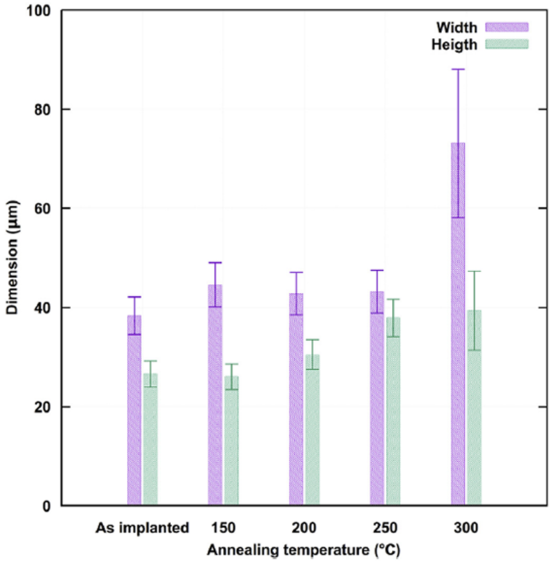
5.1. Implantation through a Silicon Mask

Both AFM and Dectac Profilometer measurements were performed on the channel waveguides fabricated in the Er-Te glass by 1.5 MeV N+ ion implantation through a special silicon mask. A typical AFM image is presented in Figure 8. Note that the profile is asymmetric and there is a compaction across the channel waveguide, as well as sharp expansions at both edges.
Besides of the AFM study, systematic profilometry using a Dectac Profilometer was also performed. The results are shown in Figure 9. At the second lowest implanted fluence (1 · 1016 ions/cm2), the profile a rectangular ridge was obtained with a height of about 25 nm (250 Å). However, at higher fluences, the surface of the implanted channel waveguides forms an asymmetric wedge-shaped compaction. Its depth increases with the implanted fluence. As will be shown later in the results of the functional studies of the waveguides, the waveguide with the regular rectangular surface profile is the best one. It is rather common that, depending on the combinations of the parameters of ion beam implantation and the target, either expansion or compaction of the same target at various implanted fluences occurs [12].

5.2. Direct Writing by an 11 MeV Carbon Ion Microbeam

The ion microbeam written channel waveguides were also studied by profilometry (Bruker Dektak XT, tip radius: 5 μm) to check for possible surface relief structures. Indeed, it was found that the irradiation by focused carbon ions produced considerable swelling of the glass sample. The surface profiles of five as-implanted channel waveguides are shown in Figure 10A. The amplitude of the ridges increases with the irradiated fluence. Even a fluence of 1.07 · 1014 ions/cm2 produced a ridge of a height of 215 nm ± 20 nm. Increasing the fluence of one decade (1.0 · 1015 ions/cm2) resulted in a ridge height of ca. 1 µm. Note that the only exception is channel No. 3 (F = 5.0 · 1014 ions/cm2), since its ridge amplitude is lower than that of channel No. 2, irradiated with half of that fluence. Moreover, the ridge over channel No. 3 is wider than the other four. This can be attributed to vibrations during irradiation. However, thermal annealing greatly reduced the height of the ridges, as can be seen in Figure 10B. The height of the ridge of over the studied channel waveguide (F = 4.6 · 1014 ions/cm2), after the complete stepwise thermal annealing (as described below), was about 100 nm. In principle, such surface ridges located over the channel waveguides could either enhance or deteriorate vertical confinement in the core, but are not capable of guiding at the designed working wavelength range of these channel waveguides.

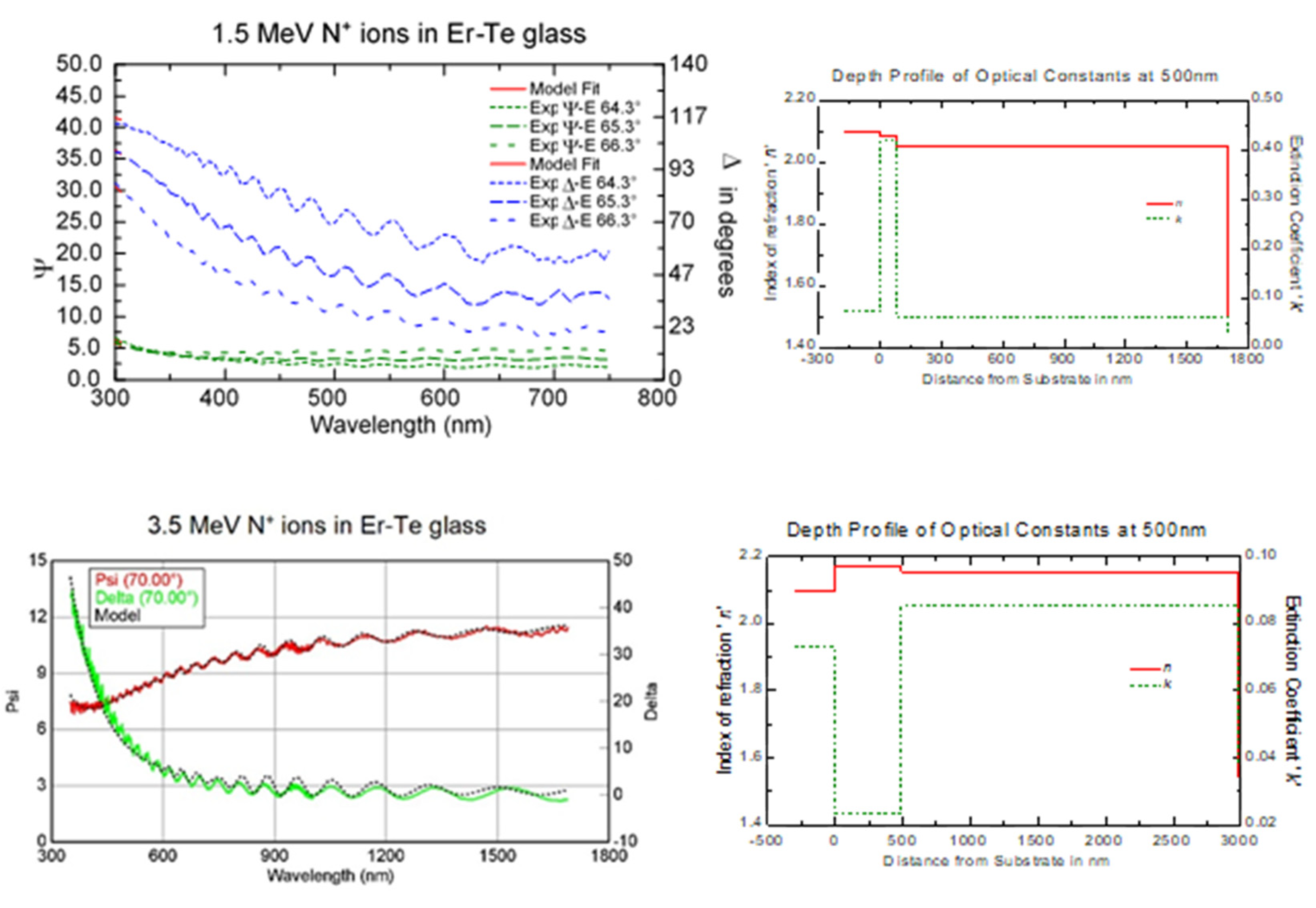
6. Spectroscopic Ellipsometry Measurements

To reveal the refractive index profile of the ion-beam-implanted channel waveguides, planar waveguides fabricated in the same material by implantation of the same ions at identical energy and fluence were studied by spectroscopic ellipsometry.
A Woollam M-2000DI spectroscopic ellipsometer was used. The parameters of the implanted planar waveguides were: implanted ions: 1.5 and 3.5 MeV N+, wavelength range: 400–1000 nm.
The optical model consisted of three layers: the stopping range (barrier), the well and the surface roughness layer. The effective medium approximation was applied [41]. The Cauchy dispersion relation was used for the description of the layers. The free parameters were the parameters of the Cauchy relation and the thickness of the layers. The WVASE32 code of Woollam Inc. was used for the evaluation of the measured spectroellipsometric (SE) data [42]. The evaluation for the planar optical waveguide implanted with 1.5 MeV N+ at a fluence of 2 · 1016 ions/cm2 yielded 4.2 ± 1.4 nm for the thickness of the surface roughness layer and 2.094 ± 0.002 for the refractive index of the non-implanted glass substrate at λ = 500 nm. The thickness of the ion stopping layer (lower layer, next to the Substrate) is 980 ± 50 nm, while the thickness of the upper layer is 1600 ± 70 nm. The refractive indices (at λ = 500 nm) are 2.15 or 2.16 (±0.01), respectively. The agreement between the ellipsometric results and the SRIM simulation are good, as can be seen in Figure 2A. Note that the ellipsometric optical model is a simplified model, containing homogeneous layers without depth inhomogeneity. (The Cauchy parameters are the followings: An1 = 1.94 ± 0.15, Bn1 = 0.09 ± 0.15, Cn1 = −0.009 ± 0.036, Ak1 = 0.023 ± 0.095, Bk1 = 0 ± 2; An2 = 1.93 ± 0.04, Bn2 = 0.086 ± 0.025, Cn2 = −0.0078 ± 0.0039, Ak2 = 0.47 ± 0.09, Bk.2 = 1.6 ± 0.3, where An, Bn and Cn are the polynomial (linear, quadratic and fourth-order) coefficients in the real part, while Ak is the amplitude and Bk is the exponent of the imaginary part of the Cauchy-formula). Results of the ellipsometric simulations for both the planar waveguides implanted with 1.5 MeV N+ at a fluence of 2 · 1016 ions/cm2 and 3.5 MeV N+ at a fluence of 4 · 1016 ions/cm2 are presented in Table 1. Note, that the modulation (the difference between the refractive index of the implanted layers and the substrate) is small, so the uncertainty of the fitted optical parameters is relatively high, see Figure 11.
Spectroscopic ellipsometry is a powerful tool for the determination of the depth distribution of refractive index in stacks of transparent thin layers. As it can see from this two examples, it can provide information on the structure and guiding capabilities of planar optical waveguides. It must be noted that m-line spectroscopy is the commonly used method to study planar waveguides [1]. In m-line spectroscopy propagation modes supported by the planar waveguide at various wavelengths are detected. Then depth distribution of the planar waveguide is determined from the detected modes. However, determination of the waveguide structure by this method is not always unambiguous. Thus, spectroscopic ellipsometric measurement of the same planar waveguide can be used to confirm the validity of the structure obtained from the m-line spectra.

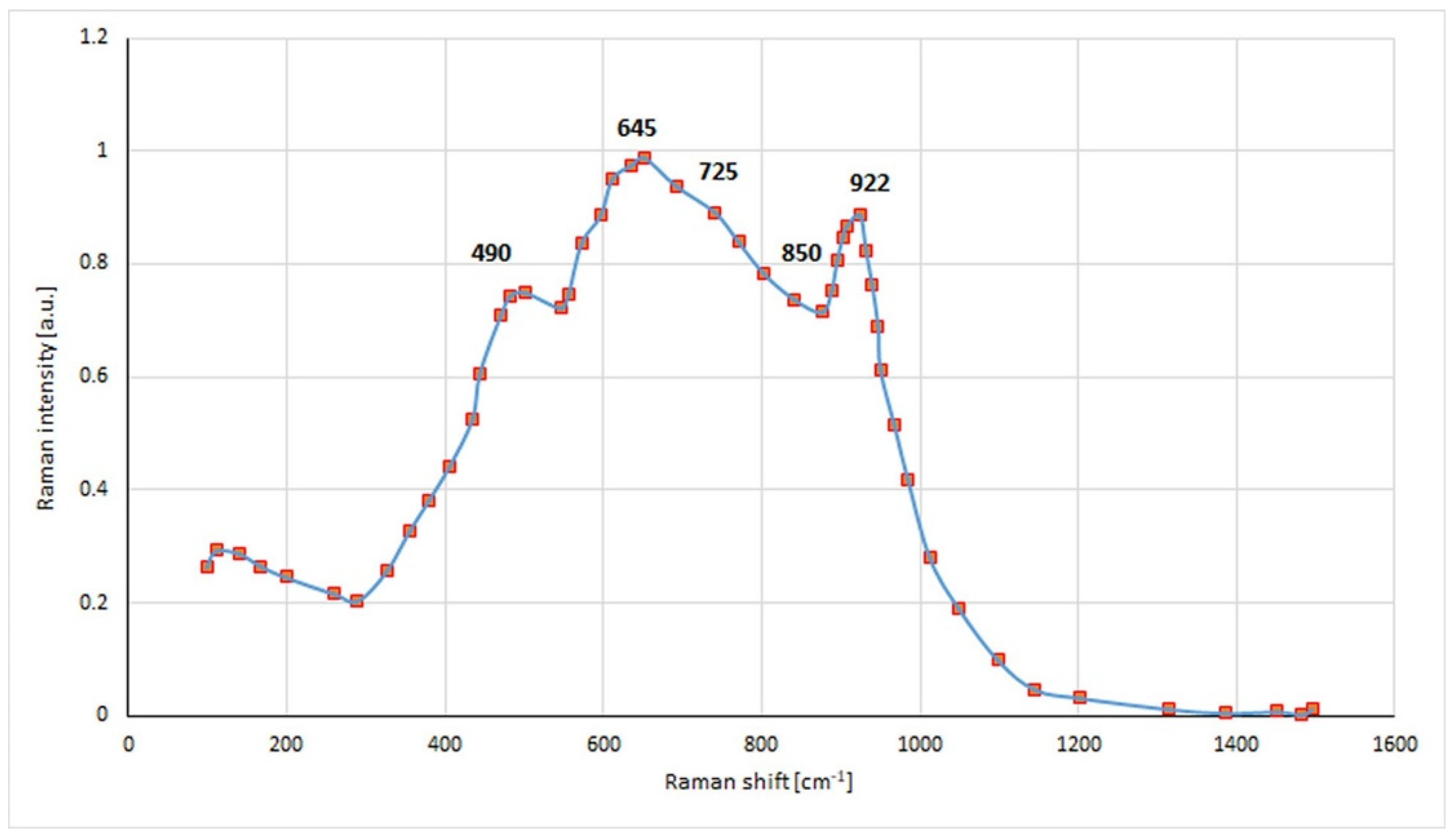
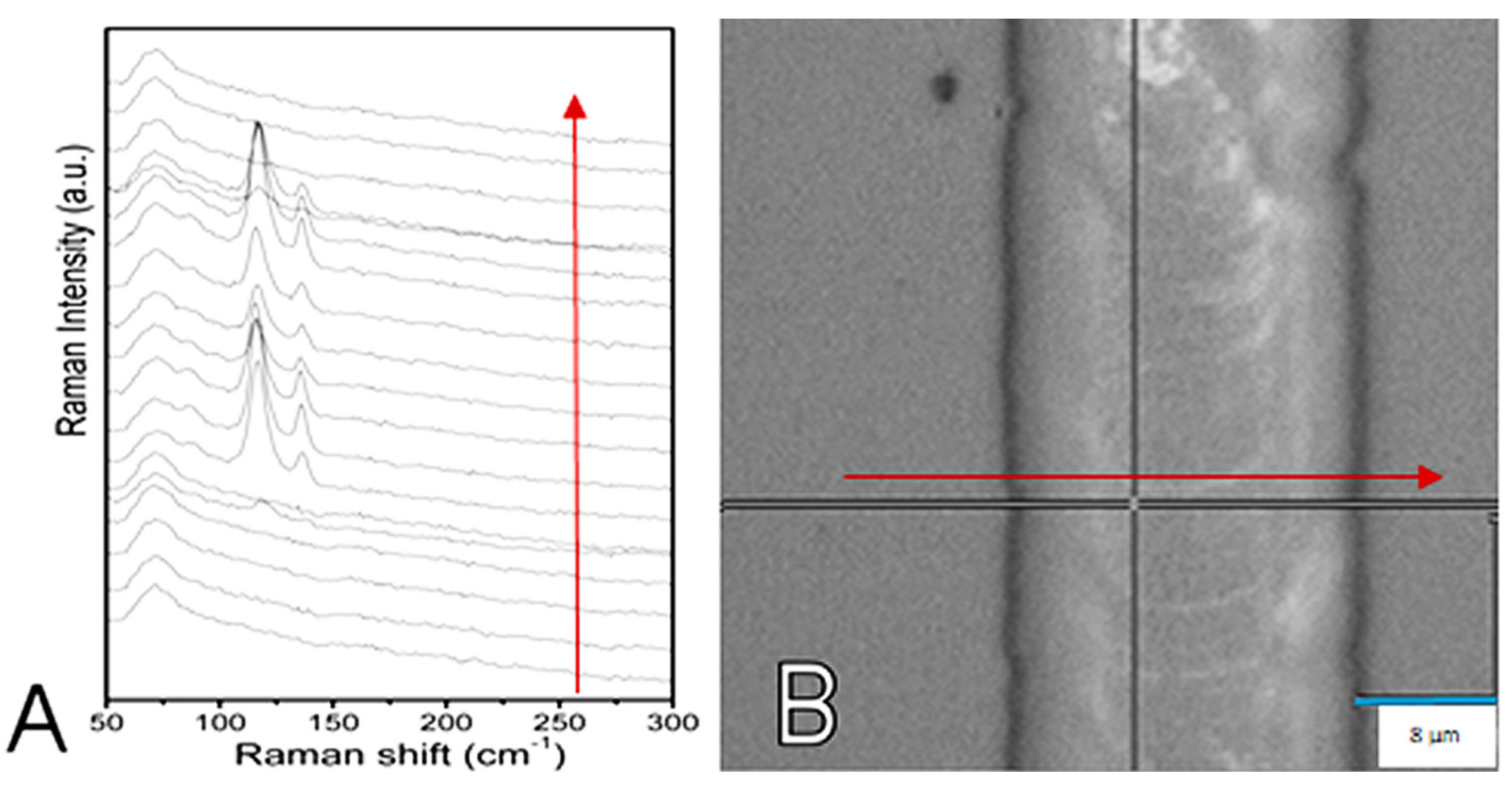
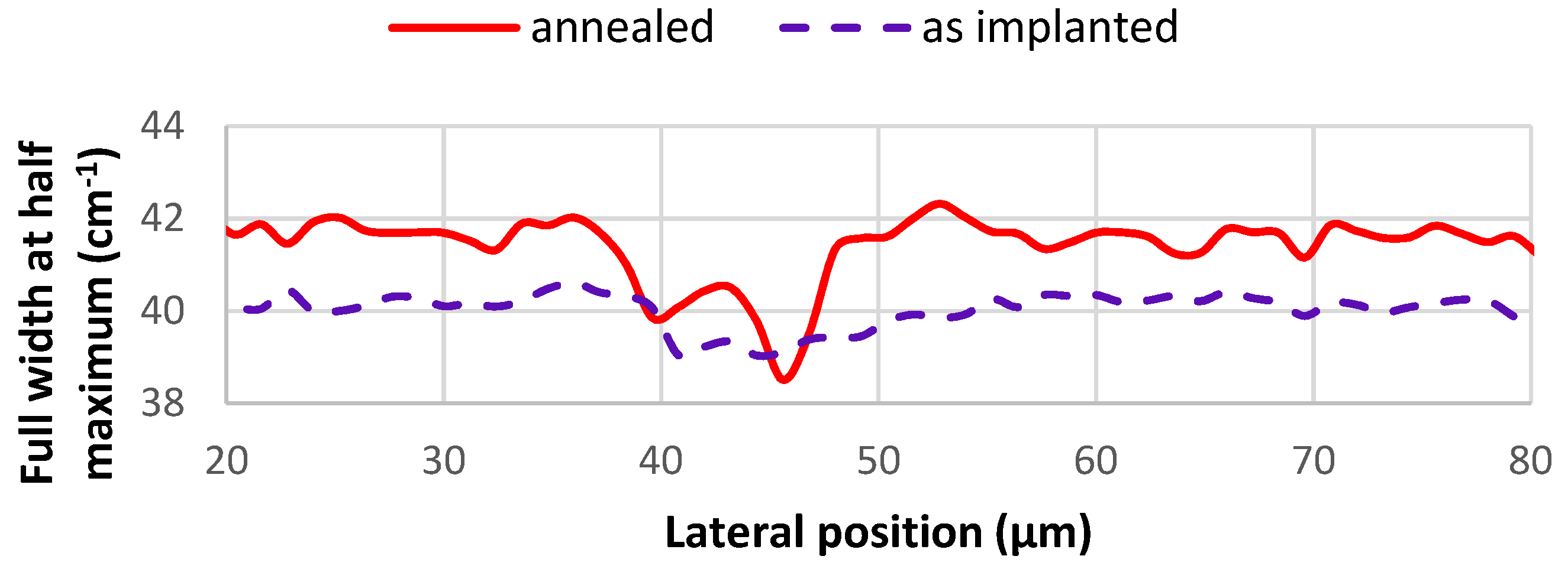
7. Micro Raman Spectroscopy

7.1. Implantation through a Silicon Mask

Raman spectroscopic measurements were performed with a Renishaw 1000 micro-Raman spectrometer at an excitation wavelength of 785 nm in order to detect the structural changes caused by the ion implantation in the channel waveguides. The Raman spectra recorded on the tellurite glass inside and outside the waveguide are shown in Figure 12.
The two spectra are very similar and resemble the Raman spectrum of tungsten-tellurite glasses. These structures are composed of tellurium-oxygen and tungsten-oxygen groups and the observed peaks can be assigned to these structural units–at 490, 645 and 725 cm−1 to the tellurite (TeO3/TeO4), and at 850 and 922 cm−1 to the tungsten oxide (WO4/WO6) [43].
The ion bombardment during the channel waveguide preparation induces only minor changes in the Raman spectrum. The most significant is the increase of the overall intensity below 300 cm−1.
A detailed Raman mapping performed perpendicular to the waveguide (Figure 13) showed, however, that more significant changes occur in the 50–300 cm−1 region. The appearance of two new Raman peaks has been observed in the implanted region at 120 and 135 cm−1. Based on their small FWHM values, these bands can be attributed to ordered (crystalline) structural units, namely, to α-TeO2 paratellurite [44] that was formed upon the ion irradiation.

7.2. Direct Writing by an 11 MeV Carbon Ion Microbeam

The Raman spectra recorded on the channel waveguides implanted with the 11 MeV carbon microbeam were very similar to those shown in Figure 12. However, new peak formation was not observed in the spectra. In contrast, changes were observed in the parameters of the peak at around 920 cm−1. Namely, the width of the band was found to decrease both in channel waveguides implanted with fluences of 4.16 · 1015 ions/cm2 (as implanted) and 4.6 · 1015 ions/cm2 (annealed) (Figure 14). This change can be attributed to an ion-beam-induced transformation (ordering) of the tungsten oxide structural units in the glass matrix. This effect is more remarkable in the annealed sample (about 3.5 cm−1 annealed vs. 1.5 cm−1 as implanted), where the heat treatment caused further relaxation (and so ordering) of the structure.

8. Functional Tests of the Channel Waveguides

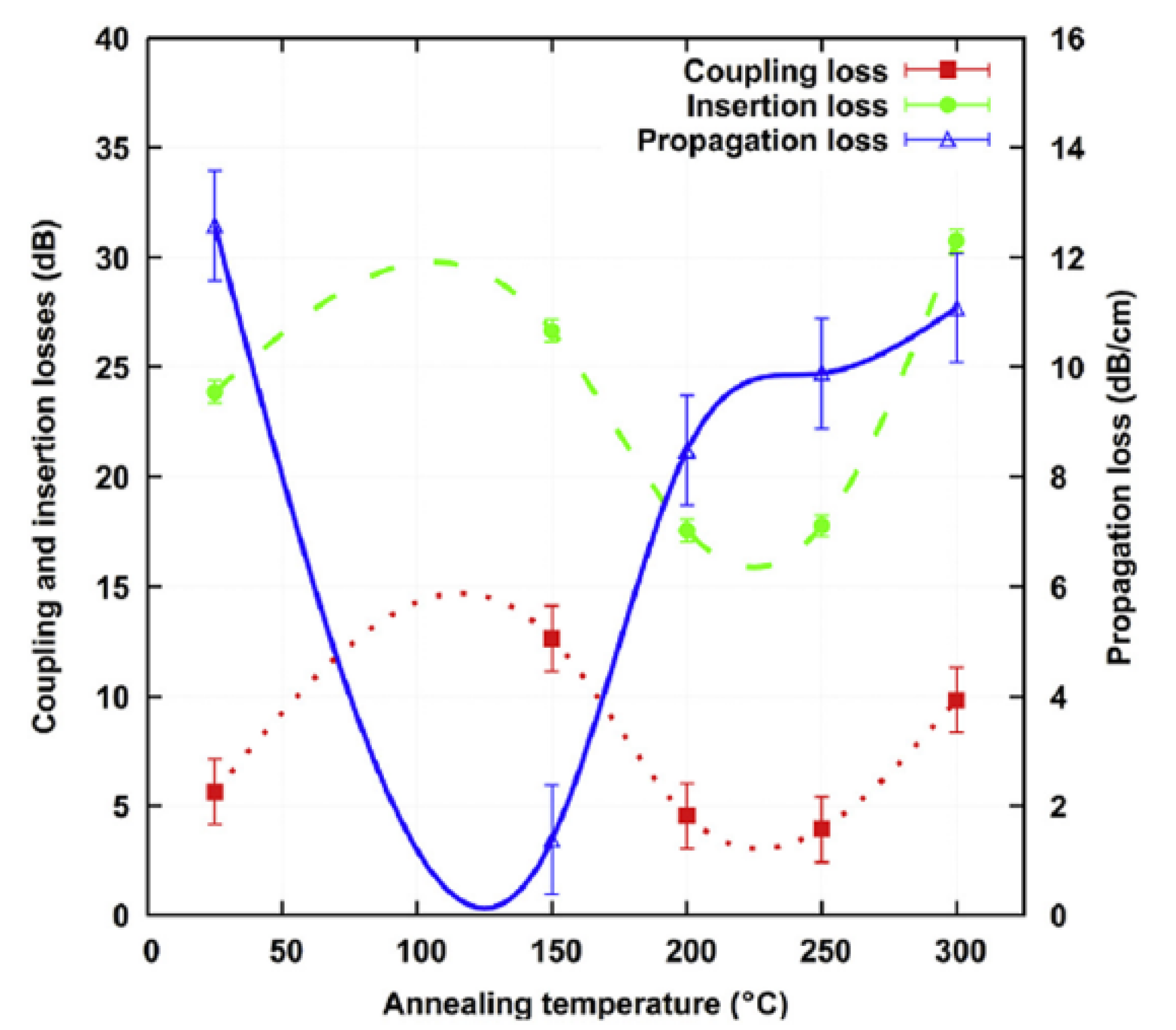
8.1. Implantation through a Silicon Mask

The guiding properties of each channel waveguide were tested. The best waveguide for E = 1.5 MeV proved to be that implanted at a fluence of 1 · 1016/cm2. Near field image emerging from the waveguide at 633 nm and green upconversion of Er3+ ions after pumping at 980 nm are shown in Figure 15. Our first results on fabrication of channel waveguides in an Er-doped Tellurite glass were published in a letter in 2007 [38].

8.2. Direct Writing by an 11 MeV Carbon Ion Microbeam

We tested wave propagation modes in each waveguide at λ = 635 nm and λ = 1540 nm. We used a special setup for propagation loss measurements. Light from tuneable diode laser sources was coupled into the channel waveguides using bare single-mode optical fibers. Thus mode size matching could be accomplished. Magnified near field images of the laser beam emerging from the channel waveguides were taken by the use of the microscope objective and a NIR sensitive Vidicon camera. Intensity of the transmitted light was measured by coupling it into another single-mode fiber and then fed into a detector. Propagation losses in both fibres, as well as insertion losses at the input and output of the channel waveguides were also measured, so that the net propagation loss could be precisely calculated. Propagation losses were measured at λ = 1400 nm. As-implanted propagation losses were rather high, between 14 and 20 dB/cm. The best channel waveguide was that implanted with a fluence of 4.6 · 1014 ions/cm2, with a propagation loss of 14 dB/cm. A stepwise annealing up to 300 °C was applied to the sample to reduce propagation losses. Results are presented in Figure 16 [40]. Propagation loss has a deep minimum around 125 °C. The lowest measured loss was 1.5 dB/cm at 150 °C, i.e., a tenfold decrease of the propagation loss was achieved.
Width and depth of the guided modes vs. annealing temperature were also measured and are presented in Figure 17. Mode depth slightly increases with temperature while the mode width does not change significantly until the 300 °C step.
In conclusion, direct writing with energetic ion microbeams proved to be a viable method for channel waveguide fabrication in tellurite glasses [40].

9. Discussion

We have demonstrated the possibility to fabricate channel waveguides in TeO2 erbium-doped glass using two methods. The first one is low-energy ion beam irradiation through a silicon mask. The second one is direct writing by microbeams of high-energy medium-mass ions The latter method allowed for lower fluences, and hence, reduced fabrication time. Besides the reduction in the necessary implanted fluence, ion microbeams also deliver very high current densities into the target, compared to those achieved by macrobeams. A region of positive refractive index change (Δn > 0) has been formed in the ion-implanted waveguide, permitting light confinement laterally and transversely. From the results obtained, it seems that ionization is the major contributing factor to the refractive index change when high-energy medium-mass ions are used.
To get a better understanding of the waveguide formation mechanism in tellurite glass, further work using FT-Raman and RNF measurements would be required.
Besides of the changes in the refractive index of the implanted regions, ridges and grooves of variable amplitude were also formed over the channel waveguides due to the ion-beam-induced expansion or compaction of the sample. Those amplitudes of the ridge and grooves were very low, between 20 and 200 nm, in the case of the 1.5 MeV N+ ion-implanted channel waveguides. In the case of 11 MeV C4+ microbeam written channel waveguides, ridge height varied between 200 and 1000 nm. However, those ridges were still not able to support guided modes, and did not affect light propagation in the channel waveguides. The large difference can be attributed to the fact that the current density in the 11 MeV C4+ microbeam was 8.70 · 10−4 A/cm2, while only 5.00 · 10−6 A/cm2 in the case of 1.5 MeV N+ ion-implanted channel waveguides.
It was found that micro Raman spectroscopy was also useful for the visualisation of structural changes in the ion-beam-implanted channel waveguides. Changes in some suitable Raman lines (line position and FWHM) correlate well with changes in the refractive index in the channel waveguides.

10. Conclusions

We have devised and realised a novel method for channel waveguide fabrication. We used high-energy microbeams of medium-mass ions for direct writing of such microstructures.
After adding a stepwise thermal annealing to the fabrication process, we achieved propagation losses down to 1.5 dB/cm, using only an implanted fluence as low as 4.6 · 1014 ions/cm2, thanks to the predominant electronic interaction at implantation.
Because of the shorter stopping range of those ions compared to MeV energy protons or He ions, we obtained channel waveguides immediately below the sample surface, in contrast to the deeply buried ones produced by the light ions. This technique hopefully makes it possible to fabricate low-loss, high-gain planar and channel-guided optical amplifiers and lasers in materials like tellurite glasses, in which it is difficult or impossible to use other techniques such as ion exchange. Such integrated optical elements could be combined with other necessary elements (possibly also fabricated using one of the here-presented ion beam techniques) to fabricate label-free optical biochemical sensors.

Author Contributions

Conceptualization, I.B.; methodology, I.B., I.R., G.U.L.N., V.H., M.F., N.Q.K. and M.V.; software, M.F.; validation, I.B.; formal analysis, I.B.; investigation, I.B., I.R., G.U.L.N., V.H., M.F., N.Q.K., V.V., Z.S., M.V., R.H., L.H. and É.T.-R.; resources, I.B., I.R., N.Q.K., V.H., M.F. and M.V.; data curation, I.B.; writing—original draft preparation, I.B.; writing—review and editing, I.B.; visualization, I.B.; supervision, I.B.; project administration, I.B.; funding acquisition, I.B., I.R. and M.F. All authors have read and agreed to the published version of the manuscript.

Funding

This study was partly supported by the RADIATE project under the Grant Agreement 824096 from the EU Research and Innovation program HORIZON 2020. The financial support of the Hungarian Government, Economic Development and Innovation Operational Program (GINOP-2.3.3–15-2016-00005) grant, co-funded by the EU is acknowledged. Partial funding from Project VOC-DETECT M-Era-Net project OTKA NNE 131269 was also received.

Institutional Review Board Statement

Ethical review and approval were not applicable.

Informed Consent Statement

Not applicable.

Data Availability Statement

Not applicable.

Conflicts of Interest

The authors declare no conflict of interest.

References

  1. Lifante, G. Integrated Photonics: Fundamentals; John Wiley and Sons Ltd.: Atrium, UK, 2003. [Google Scholar]
  2. Hunsperger, R.G. Integrated Optics: Theory and Technology; Springer: Berlin/Heidelberg, Germany, 2002. [Google Scholar]
  3. Hukriede, J.; Kip, D.; Kratzig, E. Permanent narrow-band reflection holograms for infrared light recorded in LiNbO3:Ti:Cu channel waveguides. Appl. Phys. B 2001, 72, 749. [Google Scholar] [CrossRef]
  4. Ramponi, R.; Marangoni, M.; Osellame, R. Dispersion of the ordinary refractive-index change in a proton-exchanged LiNbO3 waveguide. Appl. Phys. Lett. 2001, 78, 2098. [Google Scholar] [CrossRef]
  5. Yip, G.L.; Albert, J. Characterization of planar optical waveguides by K+-ion exchange in glass. Opt. Lett. 1985, 10, 151. [Google Scholar] [CrossRef] [PubMed]
  6. Najafi, S.I.; Touam, T.; Sara, R.; Andrews, M.P.; Fardad, M.A. Sol-Gel Glass Waveguide and Grating on Silicon. J. Lightwave Technol. 1998, 16, 1640. [Google Scholar] [CrossRef]
  7. Townsend, P.D. Development of ion implantation for optical applications. Vacuum 1998, 51, 301. [Google Scholar] [CrossRef]
  8. Yin, Z.Y.; Garside, B.K. Low-loss GeO2 optical waveguide fabrication using low deposition rate rf sputtering. Appl. Opt. 1982, 21, 4324. [Google Scholar] [CrossRef] [PubMed]
  9. Yamashiki, T.; Tsuda, K. Low-loss waveguides of benzylidene-aniline derivatives by organic molecular beam heteroepitaxy. Opt. Lett. 2003, 28, 316. [Google Scholar] [CrossRef]
  10. Wang, K.-M.; Shi, B.-R.; Cue, N.; Zhu, Y.-Y.; Xiao, R.-F.; Lu, F.; Li, W.; Liu, Y.-G. Waveguide laser film in erbium-doped by pulsed laser deposition. Appl. Phys. Lett. 1998, 73, 1020. [Google Scholar] [CrossRef]
  11. Bruno, F.; del Guidice, M.; Recca, R.; Testa, F. Plasma-enhanced chemical vapor deposition of low-loss SiON optical waveguides at 1.5-μm wavelength. Appl. Opt. 1991, 30, 4560. [Google Scholar] [CrossRef]
  12. Townsend, P.D.; Chandler, P.J.; Zhang, L. Optical Effects of Ion Implantation; Cambridge University Press: Cambridge, UK, 1994. [Google Scholar]
  13. Bindner, P.; Boudrioua, A.; Loulergue, J.C.; Moretti, P. Formation of planar optical waveguides in potassium titanyl phosphate by double implantation of protons. Appl. Phys. Lett. 2001, 79, 2558–2560. [Google Scholar] [CrossRef]
  14. Vincent, B.; Boudrioua, A.; Loulergue, J.C.; Tascu, S.; Moretti, P.; Jacquier, B.; Aka, G.; Vivien, D. Channel waveguides in Ca4GdO(BO3)3 fabricated by He+ implantation for blue-light generation. Opt. Lett. 2003, 28, 1025–1028. [Google Scholar] [CrossRef] [PubMed]
  15. Bonfigli, F.; Jacquier, B.; Montereali, R.M.; Moretti, P.; Mussi, V.; Nichelatti, E.; Somma, F. Concentration of F2 and F3+ defects in He+ implanted LiF crystals determined by optical transmission and photoluminescence measurements. Opt. Mater. 2003, 24, 291–293. [Google Scholar] [CrossRef]
  16. Szachowicz, M.; Moretti, P.; Joubert, M.-F.; Couchaud, M.; Ferrand, B. Fabrication of implanted channel waveguides in single crystal buried epitaxial layers for infrared to blue upconversion laser systems. Appl. Phys. Lett. 2007, 90, 03111. [Google Scholar] [CrossRef]
  17. Petit, V.; Moretti, P.; Camy, P.; Doualan, J.L.; Moncorgé, R. Active waveguides produced in Yb3+: CaF2 by H+ implantation for laser applications. J. Alloys Compd. 2008, 451, 68–70. [Google Scholar] [CrossRef]
  18. Buchal, C. Ion implantation for optical applications. Nucl. Instrum. Methods B 1995, 96, 370. [Google Scholar] [CrossRef]
  19. Schineller, E.R.; Flam, R.P.; Wilmot, D.W. Optical waveguides formed by proton irradiation of fused silica. J. Opt. Soc. Am. 1968, 58, 1171. [Google Scholar] [CrossRef]
  20. Meneghini, C.; le Foulgoc, K.; Knystautas, E.J.; Villeneuve, A.; Cardinal, T.; Richardson, K.A. Ion implantation: An efficient method for doping or fabricating channel chalcogenide glass waveguides. Proc. SPIE 1998, 3413, 46. [Google Scholar]
  21. Kulish, J.R.; Franke, H.; Singh, A.; Lessard, R.A.; Knystautas, E.J. Ion implantation, a method for fabricating light guides in polymers. J. Appl. Phys. 1988, 63, 2517. [Google Scholar] [CrossRef]
  22. Wilson, R.G.; Betts, D.A.; Sadana, D.K.; Zavada, J.M.; Hunsperger, R.G. Proton, deuteron, and helium implantation into GaAs and LiNbO3 for waveguide fabrication. J. Appl. Phys. 1985, 57, 5006. [Google Scholar] [CrossRef]
  23. Akano, U.G.; Mitchell, I.V.; Shepherd, F.R.; Miner, C.J.; Rousina, R. Implant-damage isolation of InP and InGaAsP. J. Vac. Sci. Technol. A 1993, 11, 1016. [Google Scholar] [CrossRef]
  24. Aithal, P.S.; Nagaraja, H.S.; Rao, P.M.; Avasthi, D.K.; Sarma, A. Effect of high energy ion irradiation on electrical and optical properties of para-hydroxy acetophenone. J. Appl. Phys. 1997, 81, 7526. [Google Scholar] [CrossRef]
  25. Szenes, G. Ion-velocity-dependent track formation in yttrium iron garnet: A thermal-spike analysis. Phys. Rev. B 1995, 52, 6154–6157. [Google Scholar] [CrossRef]
  26. Bentini, G.G.; Bianconi, M.; Correra, L.; Chiarini, M.; Mazzoldi, P.; Sada, C.; Argiolas, N.; Bazzan, M.; Guzzi, R. Damage effects produced in the near-surface region of x-cut LiNbO3 by low dose, high energy implantation of nitrogen, oxygen, and fluorine ions. J. Appl. Phys. 2004, 96, 242–247. [Google Scholar] [CrossRef]
  27. Zhu, Q.-F.; Shen, X.-L.; Zheng, R.-L.; Lv, P.; Guo, H.-T.; Li, W.-N.; Liu, C.-X. Waveguiding structures in Yb3+-doped phosphate glasses by double-energy proton and single-energy carbon-ion implantations. Mater. Res. Express 2018, 5, 016404. [Google Scholar] [CrossRef]
  28. Wang, Y.; Zhao, J.; Zhu, Q.; Shen, J.; Wang, Z.; Guo, H.-T.; Liu, C. Near-infrared carbon-implanted waveguides in Tb3+-doped aluminum borosilicate glasses. Front. Optoelectron. 2019, 12, 392–396. [Google Scholar] [CrossRef]
  29. Olivares, J.; García, G.; García-Navarro, A.; Agulló-López, F.; Caballero, O.; García-Cabañes, A. Generation of high-confinement step-like optical waveguides in LiNbO3 by swift heavy ion-beam irradiation. Appl. Phys. Lett. 2005, 86, 183501. [Google Scholar] [CrossRef]
  30. Vázquez, G.V.; Valiente, R.; Gómez-Salces, S.; Flores-Romero, E.; Rickards, J.; Trejo-Luna, R. Carbon implanted waveguides in soda lime glass doped with Yb3+ and Er3+ for visible light emission. Opt. Laser Technol. 2016, 79, 132–136. [Google Scholar] [CrossRef]
  31. Roberts, A.; von Bibra, M.L. Fabrication of Buried Channel Waveguides in Fused Silica Using Focused MeV Proton Beam Irradiation. J. Lightwave Technol. 1996, 14, 2554–2557. [Google Scholar] [CrossRef]
  32. Bettiol, A.A.; Rao, S.V.; Teo, E.J.; van Kan, J.A.; Watt, F. Fabrication of buried channel waveguides in photosensitive glass using proton beam writing. Appl. Phys. Lett. 2006, 88, 171106. [Google Scholar] [CrossRef]
  33. Liu, K.; Pun, E.Y.B.; Sum, T.C.; Bettiol, A.A.; van Kan, J.A.; Watt, F. Erbium-doped waveguide amplifiers fabricated using focused proton beam writing. Appl. Phys. Lett. 2004, 84, 684–686. [Google Scholar] [CrossRef]
  34. An, Q.; Cheng, C.; Vanga, S.K.; Bettiol, A.A.; Chen, F. Proton Beam Writing of Chalcogenide Glass: A New Approach for Fabrication of Channel Waveguides at Telecommunication O and C Bands. J. Lightwave Technol. 2014, 32, 4365–4369. [Google Scholar] [CrossRef]
  35. Yao, Y.; Tan, Y.; Dong, N.; Chen, F.; Bettiol, A.A. Continuous wave Nd:YAG channel waveguide laser produced by focused proton beam writing. Opt. Express 2010, 18, 24516–24521. [Google Scholar] [CrossRef]
  36. Bányász, I.; Fried, M.; Dücső, C.; Vértesy, Z. Recording of transmission phase gratings in glass by ion implantation. Appl. Phys. Lett. 2001, 79, 3755–3757. [Google Scholar]
  37. Bányász, I.; Berneschi, S.; Khánh, N.Q.; Lohner, T.; Lengyel, K.; Fried, M.; Péter, Á.; Petrik, P.; Zolnai, Z.; Watterich, A.; et al. Formation of slab waveguides in eulytine type BGO and CaF2 crystals by implantation of MeV nitrogen ions. Nucl. Instrum. Methods Phys. Res. Sect. B Beam Interact. Mater. At. 2012, 286, 80–84. [Google Scholar] [CrossRef]
  38. Berneschi, S.; Conti, G.N.; Bányász, I.; Watterich, A.; Khanh, N.Q.; Fried, M.; Pászti, F.; Brenci, M.; Pelli, S.; Righini, G.C. Ion beam irradiated channel waveguides in Er3+- doped tellurite glass. Appl. Phys. Lett. 2007, 90, 121136. [Google Scholar] [CrossRef]
  39. Ziegler, J.F.; Biersack, J.P. SRIM—The stopping and range of ions in matter. Nucl. Instrum. Methods Phys. Res. Sect. B 2010, 268, 1818–1823. [Google Scholar] [CrossRef]
  40. Bányász, I.; Szilágyi, E.; Rajta, I.; Nagy, G.U.L.; Pelli, S.; Comti, G.N.; Berneschi, S.; Havránek, V.; Vosecek, V.; Nagy, N.; et al. Fabrication of low loss channel waveguide in tungsten-tellurite glass by 11 MeV carbon ion microbeam for telecom C band. Opt. Mater. X 2019, 4, 100035. [Google Scholar] [CrossRef]
  41. Aspnes, D.E. Optical properties of thin films. Thin Solid Film. 1982, 89, 249–262. [Google Scholar] [CrossRef]
  42. Woollam Co., Inc. 645 M Street Suite 102 Lincoln, NE 68508 USA. Available online: http://www.jawoollam.com (accessed on 16 August 2022).
  43. Upender, G.; Sathe, V.G.; Mouli, V.C. Raman spectroscopic characterization of tellurite glasses containing heavy metal oxides. Phys. B 2010, 405, 1269–1273. [Google Scholar] [CrossRef]
  44. Sekiya, T.; Mochida, N.; Ohtsuka, A.; Tonokawa, M. Normal vibrations of two polymorphic forms of TeO2 crystals and assignments of Raman peaks of pure TeO2 glass. J. Ceram. Soc. Jpn. 1989, 97, 1435–1440. [Google Scholar] [CrossRef]
Figure 1. Fabrication of the channel waveguides by ion beam implantation through a silicon mask.
Chemosensors 10 00337 g001
Figure 2. Depth distribution of the N+ ions implanted in Er-Te glass calculated with the SRIM code. (A). E = 1.5 MeV Blue bars: Boundaries of barrier layer calculated from a spectroscopic ellipsometric (SE) measurement, see Figure 11. Implanted fluence = 2 · 1016/cm2. (B). E = 3.5 MeV. Green bars: Boundaries of barrier layer calculated from a spectroscopic ellipsometric measurement. Implanted fluence = 4 · 1016/cm2.
Chemosensors 10 00337 g002
Figure 3. Electronic (red line) and nuclear (dotted blue line) energy loss vs. depth in an Er: tungsten-tellurite glass irradiated with 11 MeV C4+ ions. Note that nuclear energy loss was multiplied by 10 for better visibility [40].
Chemosensors 10 00337 g003
Figure 4. Polarisation microscopic photos of channel waveguides implanted through a silicon mask using 1.5 MeV N+ ions at fluences of 0.5, 1, 2 and 4 · 1016 ions/cm2 (AD). Width of the channel waveguides is 25 µm.
Chemosensors 10 00337 g004
Figure 5. Polarisation microscopic photos of channel waveguides using a microbeam of 11 MeV C4+ ions at fluences of 2, 1.4, 1.4 and 0.46 · 1015 ions/cm2 (from top to bottom). Width of the channel waveguides is 15 µm.
Chemosensors 10 00337 g005
Figure 6. Interference phase contrast microphoto of parts of four channel waveguides written in an Er: tungsten-tellurite glass with a microbeam of 11 MeV C4+ ions. Irradiated fluence of the lowermost channel was 4.6 · 1014 ions/cm2, and 1.4 · 1014 ions/cm2 for the others.
Chemosensors 10 00337 g006
Figure 7. Interference phase contrast microphoto of the end face (in the centre of the image) of a channel waveguide written in an Er: tungsten-tellurite glass with a focused beam of 11 MeV C4+ ions. Irradiated fluence was 4.6 · 1014 ions/cm2. Width of the rectangular channel waveguide is 15 µm. Depth of channel waveguide is about 3.3 µm, which agrees well with the predicitons made from the SRIM simulations presented in Figure 3. A Zeiss Peraval microscope was used.
Chemosensors 10 00337 g007
Figure 8. AFM map (A) and profile (B) of a channel waveguide implanted through a silicon mask using 1.5 MeV N+ ions.
Chemosensors 10 00337 g008
Figure 9. Profiles of a channel waveguide implanted through a silicon mask using 1.5 MeV N+ ions. Fluences were 1 · 1016 (A), 2 · 1016 (B) and 4 · 1016 ions/cm2 (C).
Chemosensors 10 00337 g009
Figure 10. Surface profile of channel waveguides (A): As implanted. E = 11 MeV. Irradiated fluences from left to right: 1.0 · 1014 ions/cm2, 2.54 · 1014 ions/cm2, 5.0 · 1014 ions/cm2, 1.0 · 1015 ions/cm2 and 1.5 · 1015 ions/cm2. (B): After stepwise thermal annealing up to 300 °C. E = 11 MeV. Irradiated fluences from left to right: 1.4 · 1014 ions/cm2, 1.4 · 1014 ions/cm2 (the fluence was the same) and 4.6 · 1014 ions/cm2 [40].
Chemosensors 10 00337 g010
Figure 11. Measured (dotted) and fitted (solid lines) ellipsometric spectra (left column); refractive index (solid line) and extinction coefficient (dotted) depth-profile at λ = 500 nm (right column), calculated from the measured ellipsometric spectra of the left column. Ions: 1.5 MeV (upper row) and 3.5 MeV (lower row) N+ ions in Er-Te glass. Position and width of barrier layers, shown in Figure 2A,B were taken from the depth profile of refractive index in the right column of Figure 11.
Chemosensors 10 00337 g011
Figure 12. Raman spectra of the tungsten-tellurite glass recorded inside (red squares) and outside (blue line) the waveguide.
Chemosensors 10 00337 g012
Figure 13. Micro-Raman spectra (A) taken across a channel waveguide (B) fabricated in an Er3+- doped Tellurite glass with 3.5 MeV N3+ ion irradiation through a silicon mask. Length of the blue bar in (B) is 8 µm. The red arrows show the direction of the Raman mapping along a line perpendicular to the waveguide (B) and the order of the corresponding Raman spectra (A). Note the appearance of two new Raman peaks in the implanted region, i.e., across the channel waveguide.
Chemosensors 10 00337 g013
Figure 14. Full width at half maximum of the 922.3 cm1 Raman line across an as-implanted (dashed line) channel waveguide, irradiated with a carbon microbeam of E = 11 MeV at a fluence of 4.16 · 1015 ion/cm2, and a thermally annealed (continuous line) channel waveguide, irradiated with a carbon microbeam of E = 11 MeV at a fluence of 4.6 × 10¹⁵ ion/cm2. Note that the widths of the two channel waveguides are different [40].
Chemosensors 10 00337 g014
Figure 15. (Left): channel waveguide near field image taken at 633 nm. (Right): Green upconversion at 980 nm observed in the same waveguide. The channel waveguide is fabricated with N3+ ion at E = 1.5 MeV and F = 1 · 1016 ions/cm2 [38].
Chemosensors 10 00337 g015
Figure 16. Losses vs. temperature of the 30-min annealing steps measured at 1400 nm. F = 4.6 · 1014 ions/cm2 [40].
Chemosensors 10 00337 g016
Figure 17. Dimensions of the guided mode vs. annealing temperature. F = 4.6 · 1014 ions/cm2 [40].
Chemosensors 10 00337 g017
Table 1. Optical parameters from the SE evaluation.
Implant Energy [MeV]Thlower [nm]An1Bn1Cn1Ak1Bk1Thupper [nm]An2Bn2Cn2Ak2Bk2Thsr [nm]
1.579 ± 62.005 ± 0.010.016 ± 0.0070.0011 ± 0.0013.9 ± 1.42.1 ± 0.31620 ± 32.00 ± 0.0030.0056 ± 0.0010.002 ± 0.00010.31 ± 0.041.5 ± 0.157.6 ± 0.1
3.5489 ± 101.931 ± 0.0010.078 ± 0.001−0.0041 ± 0.00020.4 ± 0.011.36 ± 0.042381 ± 61.926 ± 0.0080.09 ± 0.02−0.023 ± 0.0070.019 ± 0.0180 ± 0.40 ± 0.3
Publisher’s Note: MDPI stays neutral with regard to jurisdictional claims in published maps and institutional affiliations.

