

Abstract
The optimization of the triboelectric layer is of paramount importance for the improvement of the performance of triboelectric nanogenerators (TENGs). In this work, we present an innovative approach exploiting the addition of highly electronegative fluorine-doped reduced graphene oxide (F-RGO) flakes into a polydimethylsiloxane (PDMS) polymeric matrix acting as the tribonegative frictional layer. The resulting layer (F-RGO/PDMS) is incorporated into a vertical contact-separation mode TENG. The optimization of the F-RGO/PDMS composition, with a F-RGO content of 2%, delivered a ten times higher power density peak compared to a F-RGO-free device. The outstanding enhancement of the power density peak is attributed to the synergistic effect of the high electronegativity of the fluorine atoms and the triboelectric properties of the graphene-based flakes. Endurance tests confirmed the stability of the F-RGO/PDMS system, demonstrating its suitability for long-lasting TENG-based wearable devices.
Export citation and abstract BibTeX RIS
1. Introduction
Recently, strong research effort has been focused on the development of clean and portable technologies, e.g. fuel cells [1], lithium-ion batteries [2] or photovoltaic solar cells [3, 4], from abundant energy sources, such as solar, thermal, wind and mechanical energies [5–7]. These efforts are needed to overcome the problems derived from the use of fossil fuels, namely the increase of CO2 emissions and depletion of oil reserves [8]. Among these environmentally friendly technologies, triboelectric nanogenerators (TENGs) have been recently developed as power devices that can effectively convert the mechanical energy into electricity exploiting both tribo-electrification and electrostatic induction [9–13]. In addition, TENGs can be easily incorporated into wearable devices as a self-powered technology [14], due to their flexibility [15], light-weight [16], low cost and easy fabrication [17]. In this context, the normal body movements (such as walking or running) generate vibrations and deformations on the clothes that can trigger a response in the form of power generation [18]. More generally, TENGs can be consireded as a part of a new class of self-powered systems, which include devices based in the piezoelectric effect [19–21].
Different TENG design configurations are proposed, namely vertical contact-separation mode (VCSM) [22], lateral contact-sliding mode [23], single-electrode mode (SEM) [24] and freestanding triboelectric-layer mode [25], being the first ones the most widely investigated due to their simplicity and facility to be integrated into flexible devices [26, 27]. Whatever is the configuration, a thorough design of the tribonegative layer, including the choice of the materials, composition and morphology, is crucial to ensure a high triboelectrification, i.e. the separation process of positive and negative charges induced by friction or interaction when in contact with the positive electrode [28, 29].
Among the different tribonegative materials, polydimethylsiloxane (PDMS), a silicone-type polymer, is one of the most used due to its position in the negative side of the triboelectric series [30]. Moreover, PDMS shows other properties, such as non-toxicity and flexibility, which are beneficial for its application in flexible and wearable devices [31]. In spite of the excellent performance demonstrated by pristine PDMS-based TENGs [32–37], numerous studies have reported that the addition of different components embedded into a PDMS matrix can improve the TENG performance compared to their equivalent additive-free PDMS-based devices [15, 38–44]. Despite the reported advances, there are still open issues to be faced in PDMS-based TENGs. One is related to the long-term storage capacity of the triboelectric layer, since its ability to store negative charges tends to decrease gradually [28]. Another limitation concerns the fact that PDMS layers offer a flat contact surface with the positive electrode, thus limiting the potential difference in the interface [45]. In order to address these problems, different graphene-related materials have been proposed as additives in the triboelectric layer [46–53]. Crumpled graphene has been incorporated onto the PDMS layer [46, 47], yielding a 20 times higher power density output, compared to that of graphene [46]. A different strategy was proposed by Hu et al, embedding aligned graphene flakes into the PDMS layer, yielding a current output 3 times higher compared to TENG based on pure PDMS [48]. This improvement is attributed to larger capacitance and lower dielectric loss due to the oriented distribution of graphene flakes [48]. Apart from pristine graphene, embedding reduced graphene oxide (RGO) in the friction layer has been also proposed as a strategy to increase the capacity of the triboelectric layer to capture and store the negative charges, resulting in the suppression of the triboelectric capacity loss of the polymeric layer [49].
With regard to the different graphene-derivatives, graphene oxide (GO) has been reported as a promising additive in PDMS-based TENG systems [50–52]. As an example, Kang et al investigated the triboelectric activity of GO-filled PDMS composites, concluding that the superior performance yielded by the GO/PDMS composite compared to GO-free PDMS (with values of voltage and current output 3-fold higher) is attributable to the highly electronegative oxygen functional groups of GO, such as epoxy, hydroxyl and carboxylic acid groups [50]. This finding suggests that the presence of highly electronegative elements in combination with the properties of graphene-derivatives may also have a positive impact on the triboelectric activity. In fact, the capacity of highly electronegative atoms to attract electrons from the electropositive side favours the electrostatic induction in TENG systems [54], being the generation of triboelectric charges closely related to the difference of electronegativity of the two triboelectric layers [55]. In this context, fluorine is the most electronegative element due to its strong capacity to attract electrons to fill its valence shell, following the octet rule [56]. Polymeric materials containing fluorine in their composition, such as polytetrafluoroethylene (PTFE) [44, 57, 58] and polyvinylidene fluoride (PVDF) [59–61], have been widely reported as triboelectrically active materials for TENGs. Nevertheless, both materials present several issues. In fact, PVDF shows a lower absolute value of triboelectric charge density compared to PDMS (87.4 ± 2.1 vs 102.1 ± 2.2 µC m−2, respectively) [30], whereas PTFE requires strict conditions for its synthesis and processing, being also not suitable for flexible devices due to its stiffness and low flexibility [62].
In the present work, we propose an alternative strategy to add fluorine into the triboelectric layer. The incorporation of this element into the graphene-based structure is carried out by chemical doping to produce fluorine-doped reduced-graphene oxide (F-RGO) [63], which has been previously investigated for different applications [64–66]. Nevertheless, to the best of our knowledge F-RGO has not been reported for its application in TENGs so far. The addition of F-RGO flakes into a PDMS-based electronegative layer determined a 10-fold power density enhancement (keeping its voltage output after 4000 cycles of continuous operation) compared to the F-RGO-free VCSM TENG. The mechanism behind this enhancement is attributed to the synergistic effect between the high electronegativity of the fluorine atoms and the triboelectric properties of the graphene-based flakes. This result suggests the high capacity of F-RGO to act as an electron trapping material, a behaviour which has been previously reported in a RGO-based TENG [49].
2. Results and discussion
2.1. Characterization of F-RGO flakes
The synthesis of F-RGO from RGO was carried out by a fluorination process following the procedure described in the Methods section. Before its incorporation into the polymeric matrix, the as-produced F-RGO material was fully characterized, and the results are presented here. First, the morphology of the F-RGO flakes was characterized by TEM, and the corresponding image is shown in figure 1(a). It is observed a characteristic silk veil-like RGO nanosheet, with a wrinkled shape morphology. From the different TEM images obtained, the average lateral size of the F-RGO flakes is determined to be >1 µm. The inset in figure 1(a) reveals the selected area electron diffraction (SAED) pattern, in which well-defined rings characteristic of <0001>-oriented graphite can be identified [67]. Nevertheless, the SAED pattern observed here differs significantly from that reported for individual graphene sheets [68] due to the doping, layer overlapping [69, 70] and the amorphous structure [71, 72], which is a consequence of the fluorination process [73]. The morphology of the F-RGO flakes was further evaluated using atomic force microscopy (AFM) (figure 1(b)), providing a thickness of the F-RGO flake of ∼5 nm. The thickness of one fluorinated graphene layer has been demonstrated to be 0.62 nm by theoretical calculations [74]. Nevertheless, AFM measurements of F-RGO monolayers have reported higher values in the order of 0.8–0.9 nm [75, 76], being the difference compared to the theoretical calculation attributed to the van der Waals radius of fluorine (0.147 nm) [77]. Therefore, it can be concluded that the F-RGO flakes synthesized in this work are constituted by ∼5–6 individual layers.

Figure 1. (a) BF-TEM image of a F-RGO flake. Inset: Corresponding SAED pattern, according with mutually in-plane-rotated [0001]-oriented graphene flakes (graphite 2H, ICSD 230104). (b) AFM image and cross-sectional analysis of a few-layered F-RGO sample deposited on a Si substrate. (c) ADF-STEM image of a flake in the F-RGO sample, suspended on a holey C-film, and (d), (e) STEM-EDS elemental mapping showing the distribution of C and F, respectively. (f) Corresponding EDS spectra obtained on a region of the same flake entirely suspended on a hole.
Download figure:
Standard image High-resolution imageThe elemental distribution was investigated by STEM-EDS and the elemental mapping is shown in figures 1(c)–(e). It is observed that F is uniformly distributed throughout the flake, thus confirming the homogeneity of the sample. The EDS spectra displayed in figure 1(f) confirms that fluorine is present in the sample (8.0%), as well as minor amounts of oxygen (1.6%), nitrogen (0.5%) and traces of sulfur (<0.1%) remaining from the GO synthesis. The chemical composition of the synthesized F-RGO was further investigated by high-resolution x-ray photoelectron spectroscopy (XPS) measurements.
Figure 2(a) shows the XPS survey spectra, in which the characteristic C 1s, O 1s and F 1s peaks are observed at 284.5, 533.0 and 687.0 eV, respectively [76]. From the area under each peak the composition is calculated to be 77.0% of C, 20.1% of F and 2.9% of O, being the C/F ratio 3.83. It should be noted that a difference emerges in the values of F content yielded by STEM-EDS and XPS analysis. This discrepancy can be explained by the different nature of both techniques. Considering that we are dealing with F-RGO flakes conformed by several layers, it is probable that the incorporation of F atoms during the fluorination process takes place mainly on the surface of the RGO flakes, whereas a relatively lower amount of F species is accommodated in the interlayer space between adjacent RGO layers. The consequence is that a surface analysis technique such as XPS yields a higher fluorine content than a bulk technique such as EDS. The incorporation of fluorine into the graphene structure is confirmed by the presence of the single and symmetric F 1s deconvolution peak (figure 2(b)) observed at 686.8 eV, being this position ascribed to semi-ionic C–F bonds (687.5 eV) rather than covalent C–F bonds (688.6 eV) [78]. In figure 2(c) it can be seen the C1s deconvolution peak, which shows a distortion due to the addition of the fluorinated species and can be deconvoluted into the following carbon bonding moieties: C=C (at 284.5 eV), C–C/C–H (285.5 eV), C–O/C=O (286.7 eV), C–F (288.3 eV), O–C=O (289.4 eV), C–F2 (290.2 eV) and C–F3 (293.0 eV) [76]. The carbon–fluorine bonds represent 35.9% of the total bonds involving the C atoms, which can be split into 21.8% for C–F, 11.7% for C–F2 and 2.4% for C–F3, while the carbon-oxygen species account for only 8.7%. These oxidized carbon species are present mainly as carbonyl and epoxy moieties representing the peak at 286.7 eV, whereas the peak at 289.4 reflects a minor presence of carboxyl groups, compared to the other two species [76]. To confirm these results, Fourier-transform infrared (FTIR) measurements were carried out under the reflectance mode, as shown in figure 2(d). A wide region ranging from 900 to 1400 cm−1 with a peak at 1053 cm−1 is observed, that is close to the value of 1084 cm−1 reported for semi-ionic stretching vibrations of C–F bonds [79], whereas the shoulder observed at 1221 cm−1 is attributed to the presence of covalent C–F bonds [80]. This occurrence of the semi-ionic C–F species over the covalent C–F bonding confirms the conclusions obtained from the analysis of the F 1s deconvolution peak in XPS analysis. The vibration band observed at 1579 cm−1 reflects the presence of C=C bonding species [81], while the weak peak at 1730 cm−1 confirms the marginal presence of C=O moieties [82] compared to C–C and C–F species.

Figure 2. (a) Wide XPS survey spectra of F-RGO. XPS core levels of (b) F 1s and (c) C 1s deconvolution peaks. (d) FTIR spectra of F-RGO. (e) XRD patterns of GO, pristine Graphene and F-RGO. (f) Raman spectra of F-RGO using an excitation laser wavelength of 532 nm. Inset: distribution of ID/IG calculated ratios.
Download figure:
Standard image High-resolution imageTo obtain information about the structure of the F-RGO and more precisely concerning the interlayer distance between adjacent graphene layers, x-ray diffraction (XRD) diffraction measurements were carried out. Considering the values of 2θ at which the (002) diffraction peaks arise, the interlayer space can be calculated using the Bragg's equation [83]. Figure 2(e) reflects that the peaks corresponding to (002) reflection appear at values of 2θ equals to 10.6° for the GO precursor and 26.1° for a standard pristine graphene sample, corresponding to interlayer spaces of 0.83 nm [84] and 0.34 nm [85], respectively. The (002) diffraction peak for F-RGO appears at 15.6°, corresponding to a calculated interlayer distance of 0.57 nm, an observation in agreement with theoretical calculations, in which the interlayer distance in graphite fluorides is calculated to be around 0.61 nm in the case of C–F bonding species predominance [74].
The interlayer space between graphene layers is linked to the amount of doping species present [71], therefore the value obtained for F-RGO (20.1% F content) is an intermediate value between pristine graphene and GO (42% O content), as expected. In addition, the (100) reflection is observed at 2θ = 42.7°, but there is no peak at 2θ = 44.5° corresponding to (101) reflection. The (100) peak has been ascribed to reflections in the carbon phase due to the presence of dopant species [86]. Raman measurements of F-RGO were also performed using a 532 nm laser and the results are displayed in figure 2(f). Raman spectroscopy is a useful tool to characterize carbon-based nanomaterials and hybrid structures [87, 88]. The typical Raman spectrum of F-RGO consists of two distinctive bands characterized by G peak at 1584 cm−1, which corresponds to the E2g phonon of the sp2 carbon atoms, and D peak at 1345 cm−1, which represents sp3 hybridized carbon atoms indicating the presence of lattice distortions. Therefore, the intensity ratio of the D and G bands (ID/IG) provides a measurement of the defects present in the graphene structure [89]. The inset of figure 2(f) displays the Gaussian distribution of the calculated ID/IG ratios having an average value of 1.04, meaning that the doping procedure altered the structure of F-RGO [90]. The Raman spectrum also shows the presence of the 2D peak at 2679 cm−1 and the combination mode D + G at ∼2965 cm−1.
2.2. Device description and TENG operation
The synthesized F-RGO flakes were embedded into the PDMS polymeric matrix with an F-RGO content of 2 wt.% with respect to PDMS and incorporated into the VCSM TENG as represented in the schematic illustration of figure 3(a). The bottom part of the TENG was formed by the poly(methyl methacrylate) (PMMA) acrylic substrate/Al electrode/(F-RGO/PDMS) triboelectric layer, in which the latter was acting as the negative friction material.

Figure 3. (a) Schematic illustration of the vertical-contact separation mode TENG. Inset: schematic view of the electron transfer from the PDMS matrix to the F-RGO lattice. (b) Picture of the TENG device used in the experiments. (c) Picture of the F-RGO/PDMS triboelectric layer.
Download figure:
Standard image High-resolution imageInstead, the top part consisted of the PMMA acrylic substrate/Al electrode with the Al foil acting simultaneously as the positive layer and the metal collector. A picture of the device can be observed in figure 3(b), whereas figure 3(c) shows the flexibility of the F-RGO/PDMS triboelectric layer. For comparison purposes, an identical TENG was fabricated with pristine PDMS (without the F-RGO material) as the triboelectrically negative layer. Both PDMS layers were produced using the Doctor Blade technique as described in the Experimental section, yielding polymeric membranes with a thickness of 304 ± 6 µm. This value was measured by screw gauge and was confirmed by cross-sectional images obtained by optical microscopy at different points of the polymeric layer. In addition, the positive part of the TENG was shared for the tests of the two different triboelectronegative layers to facilitate the comparison.
Once the TENG device is assembled a motor provides the external press and release forces that generate the contact and separation between the two parts of the TENG, as shown in figure 4(a). At the starting point, the top and bottom parts of the TENG are at the maximum spatial separation, there being an electrostatic equilibrium between the tribonegative layer and the bottom Al electrode. In this situation, there is no charge transfer between the top positive electrode and the tribonegative layer due to the separation between them, reaching the output voltage its maximum value [91]. This value is the so-called open-circuit voltage (Voc), which can be expressed as [92]:
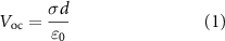

Figure 4. (a) Schematic view of a TENG contact-separation cycle under external force. (b) Output current density generated by the TENG in a full cycle.
Download figure:
Standard image High-resolution imagein which, σ is the charge density of the electroactive layer, d is the separation distance between the positive electrode and the tribonegative layer, and  0 is the vacuum permittivity. If compressive forces are applied, the interlayer distance between the top positive electrode and the triboelectric layer decreases and the system undergoes a break of the equilibrium [93].
The positive and negative charges start to build up on the surfaces of the Al electrode and the polymeric layer, respectively, and the electrons flow from the top electrode to the bottom collector through the external circuit in order to compensate the different polarity (figure 4(b)) [94]. The maximum value of the measured current is the short-circuit current density (Jsc). When the positive electrode and the triboelectric layer are in contact an electrostatic equilibrium is reached, characterized by the build-up of positive and negative charges in the Al electrode and triboelectric layer interface, respectively. This equilibrium is determined by the maximum capacity of the triboelectric layer to accept electrons from the top Al foil, which acts as the electron donor. Once the external compressive forces are released, the separation of the electro-opposite layers breaks the electrostatic equilibrium again. At this point, the negative charges start to dissipate from the top surface of the triboelectric layer towards its opposite side in contact with the bottom electrode. Consequently, the electrons flow from the bottom current collector towards the top electrode until the system reaches its original position, i.e. the maximum separation between the Al electrode and the polymeric layer. Under the action of repeated press-release forces, successive cycles take place to operate the TENG [10].
2.3. Influence of F-RGO addition on performance
The F-RGO/PDMS triboelectric layer was incorporated into the TENG as described above, being the TENG operated under external force of 10 N, frequency of 4 Hz and with maximum interlayer distance between the positive Al electrode and the negative triboelectric layer fixed at 5 mm. A F-RGO-free equivalent system was also tested for comparison. Under these conditions, the values of voltage and current density were monitored, and the results are shown in figure 5. In this context, figure 5(a) exhibits the voltage outputs, showing that the system with pristine PDMS as triboelectric layer develops a maximum VOC of 66.0 V, whereas in the case of the TENG with F-RGO/PDMS layer the VOC drastically increases to 235.6 V. According to equation (1) and considering that the interlayer distance and the vacuum permittivity were the same in both systems described above, it is concluded that the charge density is four times higher in the F-RGO/PDMS system compared to pristine PDMS. A similar response is observed in terms of JSC, as shown in figure 5(b). The maximum value of JSC observed in the pristine PDMS system is 1.89 mA m−2, which is much lower than the maximum JSC observed for the F-RGO TENG (8.47 mA m−2). It is noticeable that in both figures 5(a) and (b) the press and release peaks are not symmetric, which is due to the different nature of the phenomena taking place, i.e. contact-induced electrification and charge redistribution, respectively [95]. The measured V and J outputs of a TENG vary depending on the resistance of an applied external load. While the measured voltage increases with the value of the external resistance, the current density decreases when the magnitude of the load rises. This fact can be observed in figure 5(c), in which the values of measured V (in brown) and J (dark cyan) are plotted vs different values of external resistance for the F-RGO/PDMS system. It is observed that V starts to increase from a value of external load higher than 0.5 MΩ and reaches the VOC at ∼500 MΩ, when the J value falls to zero. On the contrary, the Jsc is measured under values of external resistance lower than 0.5 MΩ. From this graph, the power density developed by the system under the application of different external resistance loads can be calculated and plotted. The resulting power density curve is displayed in figure 5(d), with a maximum power density (Pmax) that is reached under a specific external resistance. In the case of the pristine PDMS system, the value of Pmax (34.9 mW m−2) is reached under a load of 22 MΩ, whereas the F-RGO TENG develops a Pmax of 363.3 mW m−2 (under a load of 10 MΩ), which is more than 10 times higher than in the case of its F-RGO-free counterpart.
Figure 5. (a) Voc and (b) Jsc of the PDMS and F-RGO/PDMS systems. (c) Dependence of the output V (right, in brown) and J (left, in dark cyan) on the external loading resistance for the F-RGO system. (d) Output P vs load resistance for the PDMS and F-RGO/PDMS systems.
Download figure:
Standard image High-resolution imageTo find an explanation for the 10-fold enhancement of performance shown by the F-RGO/PDMS triboelectric layer compared to pristine PDMS, several facts should be considered. First, it should be taken into account that the periodic contact-separation cycles between the electropositive Al foil electrode and the negative composite layer alternatively modify the induced potential, thus producing a flow of electrons through the external load in alternate directions [9]. Therefore, the electrostatic induction of the triboelectric layer plays a crucial role in the measured voltage and current outputs. Theoretical studies attribute electrostatic properties to graphene [96, 97], concluding that it is able to store electric charges for a decay time that can be as high as 40 min [98]. In this context, RGO has been demonstrated to be an effective electron trapping material that can improve the performance of polyimide-based triboelectric layers [49]. Moreover, the wrinkled morphology of the F-RGO nanosheets observed by TEM imaging increases the frictional surface area in the Al electrode–triboelectric layer interface, which can favor the roughness and friction of the triboelectric layer [99]. In addition, the presence of the highly electronegative fluorine atoms is linked to the triboelectric effect observed in certain polymeric materials, such as PTFE and PVDF. Since in the present study PDMS, a fluorine-free polymer, is used as the polymeric matrix, the triboelectric activity of the fluorine atoms can only come from the doping atoms present in the graphene nanosheets.
2.4. Synergistic effect of fluorine and graphene-based structure
The individual contribution of both factors described above (the electrostatic induction of graphene flakes and the electronegative activity of the fluorine atoms) on the enhanced performance is evaluated. For this purpose, the triboelectric activity of the F-RGO/PDMS system is compared with an equivalent triboelectric layer consisting of pristine graphene embedded into PDMS (Gr/PDMS), and a third composite material consisting of the commercial highly fluorinated Fluorinert® FC-40 (with a F content of ∼77 wt.%) embedded in the same PDMS matrix (FC40/PDMS), both with the same composition of F-RGO/PDMS system, viz. 2 wt.%. The V outputs measured for these three systems are shown in figure 6(a), being observed that the VOC values of FC40/PDMS and Gr/PDMS TENGs (55.7 and 80.7 V, respectively) are much lower compared to those ones measured in the F-RGO/PDMS system (235.6 V). A similar pattern is observed for the Jsc outputs (figure 6(b)), in which the value measured for F-RGO/PDMS is ∼7 times higher than those obtained for Gr/PDMS and FC40/PDMS (1.26 and 1.18 mA m−2, respectively). The curves representing the measured J as a function of the output V for the three systems are plotted in figure 6(c). From this graph, the maximum peak power density is calculated from the area of the largest rectangle defined by the V–J curve [100]. It is observed that F-RGO/PDMS yields a power density output, which is 22 and 20 times larger than the one of fluorinated FC40/PDMS layer (16.6 mW m−2) and pristine graphene Gr/PDMS system (18.5 mW m−2), respectively. These observations are in good agreement with the charge transfer calculated for the three systems, as shown in figure 6(d), being the total charge generated in a press-release cycle calculated to be 0.76 µC m−2 for FC40/PDMS, 1.54 µC m−2 for Gr/PDMS and 3.75 µC m−2 for F-RGO/PDMS.

Figure 6. (a) Voc and (b) Jsc of F-RGO/PDMS, Graphene/PDMS and Fluorinert FC-40/PDMS systems. (c) Curves of peak current density vs peak voltage measured at specific resistance values for the TENGs with F-RGO/PDMS, Gr/PDMS and FC-40/PDMS polymeric layers. The maximum peak power density can be calculated from the largest rectangle area under the curves. (d) Charge transfer generated during a press-release cycle for the three different TENGs (error bars represent the standard deviation). (e) Sketch describing the interaction between the electrons and the PDMS-based graphene, Fluorinert® FC-40 and F-RGO triboelectric systems.
Download figure:
Standard image High-resolution imageConsidering these results, it is concluded that the addition of graphene nanosheets or a fluorine-based material into the PDMS matrix has no significant influence on the triboelectric activity of the triboelectric layer compared to pristine PDMS when they are present individually. On the contrary, graphene and fluorine show an outstanding triboelectric activity when they are combined in the form of F-RGO embedded in the PDMS matrix. This finding points out that the triboelectric activity of graphene-based structure and the electron-attracting nature of fluorine are not independent phenomena, but they act synergistically in triboelectrically active systems. This synergistic effect is graphically described in figure 6(e), where it is seen how the electrons can move freely within the graphene lattice. The figure also reflects the capacity of the highly fluorinated Fluorinert® FC-40 to attract the electrons, although its insulating nature does not permit the mobility of the electrons between the molecules. In contrast, the F-RGO structure integrates the electron attraction of F atoms as a source of electrons towards the graphene-based lattice, in which an abundant cloud of electrons can move freely, resulting in the increased output voltage and current.
2.5. Influence of F-RGO content on performance
The previous results have been obtained for a F-RGO content of 2 wt.% in the PDMS matrix. In order to evaluate the influence of the amount of F–Gr on the TENG performance, four F-RGO/PDMS layers were prepared modifying the F-RGO content from 0 to 3 wt.%, which will be named thereinafter as pristine PDMS, F-RGO/PDMS 1%, F-RGO/PDMS 2% and F-RGO/PDMS 3%, respectively. The corresponding measured V, J and maximum P (Pmax) outputs are displayed in figures 7(a)–(c), respectively. It is observed that the measured V increases with the amount of F-RGO until reaching a maximum value at a composition of 2 wt.%, whereas beyond this percentage the value of the measured V decreases. The same pattern is observed in terms of J and Pmax outputs, namely maximum values are reached at a F-RGO content of 2 wt.%, whereas a decrease occurs when the amount of F-RGO rises to 3 wt.%.

Figure 7. (a) Voc and (b) Jsc of the F-RGO/PDMS TENG at different F-RGO compositions. (c) Dependence of Pmax on the F-RGO content, showing the corresponding spline fitting. (d) Charge transfer of the TENGs with different compositions (error bars represent the standard deviation). (e) Representative AFM images of pristine PDMS, F-RGO/PDMS 1%, F-RGO/PDMS 2%, and F-RGO/PDMS 3% triboelectric layers.
Download figure:
Standard image High-resolution imageIn agreement with this behavior, figure 7(d) reveals that the F-RGO/PDMS system with a F-RGO content of 2 wt.% yields a higher value of transferred charge compared to the system with a F-RGO content of 1 wt.% (i.e. 3.75 vs 3.56 µC m−2, respectively), whereas a substantial drop is observed when the F-RGO content rises to 3 wt.% (1.71 µC m−2). A similar increasing-decreasing trend has been also reported for PDMS filled with highly dielectric nanoparticles, such as SrTiO3 [42]. The improvement in triboelectric activity of the polymeric layer as the F-RGO content increases is attributed to the higher presence of electronegative F-RGO flakes. In contrast, the decrease in triboelectric activity observed beyond a composition of 2 wt.% is attributed to agglomeration of F-RGO nanosheets in the polymeric structure. To visualize the distribution of F-RGO flakes on the surface of the polymeric matrix, AFM measurements have been carried out on the triboelectric layers with different F-RGO contents, and the results are shown in figure 7(e). It is observed that the pristine PDMS sample exhibits a smooth surface (RMS roughness value of 2.1 ± 0.6 nm) due to the absence of fillers. In the case of the F-RGO/PDMS 1%, the presence of F-RGO flakes slightly increases the roughness of the surface (RMS roughness 5.1 ± 1.4 nm) compared to pristine PDMS, whereas in the F-RGO/PDMS 2% system (RMS roughness 8.7 ± 2.1 nm) a homogeneous distribution of the F-RGO flakes along the polymeric surface is seen. In contrast, when the F-RGO content is increased to 3 wt.% (RMS roughness 15.7 ± 4.7 nm) it is observed the presence of F-RGO flakes agglomeration. Significantly, the standard deviation value of RMS surface roughness abruptly increases from 2.1 nm for a F-GRO content of 2 wt.% to 4.7 nm for an F-RGO content of 3 wt.%, which provides numerical evidence of the transition to a more inhomogenehous surface. Consequently, the excessive concentration of stacked F-RGO flakes causes a disruption in the continuity of the PDMS matrix, leading to isolated polymeric zones surrounded by F-RGO flakes, which alters the insulating nature of the polymeric layer. This observation has been previously reported in PDMS matrices filled with conductive co-polymers, giving as a result discontinuous morphologies at high filling contents [101]. A complementary theory is proposed by Kim et al, who ascribed the performance decrease to the excess of RGO flakes, which determines an electric-field screening effect that can suppress the induction of positive charges at the bottom current collector [49].
2.6. Long-term operation
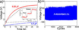
During the TENG operation, the press and release movements can be used to charge a capacitor if the output V signal is rectified. In this context, the F-RGO/PDMS 2% TENG was used to charge two capacitors with different capacities, and the results are shown in figure 8(a). The 0.22 µF capacitor was charged to 6 V in merely 15 s, whereas a 4.7 µF needed 23 s to be charged to 1 V. In the enlarged view of the 0.22 µF capacitor curve displayed in the inset of figure 8(a) both the press and release movements can charge the capacitor due to the rectification of the V output signal, thus increasing the voltage of the charged capacitor of ∼0.12 V at each step.
Figure 8. (a) Charging capability of F-RGO/PDMS 2% system with two different capacitors. Inset: enlarged view of charging process of 0.22 µF capacitor. (b) Durability test performed under compressive force of 10 N, frequency of 4 Hz and layer separation of 5 mm during 4000 continuous cycles for the F-RGO/PDMS 2% TENG system.
Download figure:
Standard image High-resolution image
A long-time test was also carried out to evaluate the durability of the material as triboelectrically active surface. Due to the working mechanism of TENGs [10] the electrons are injected from the Al foil into the polymeric layer, leaving positive charges in the metal surface. It has been theoretically demonstrated that this cyclic charge transfer may take place until a certain number of cycles, when the accumulation of charges reaches an equilibrium due to the saturation and preservation of charges on the PDMS layer due to its insulating nature [102]. The durability test was carried out for the F-RGO/PDMS 2% system under the same operational conditions reported in the previous measurements, and the corresponding results are displayed in figure 8(b). It is observed that after 4000 consecutive cycles the V output does not suffer any reduction due to saturation. Moreover, it is even increased up to 40% (327.6 V) compared to the initial measured voltage (235.6 V). This could point to the positive effect that the presence of doped graphene flakes may have in the charge redistribution within the polymeric lattice, via the modification of the insulating nature of the PDMS matrix. This result demonstrates that the performance integrity of the system is not jeopardized by continuous operation under demanding conditions, confirming that the proposed F-RGO/PDMS TENG is suitable for applications in which a stable response during long-time use is a prerequisite.
3. Conclusions
F-RGO has been synthesized and characterized for its application into a vertical contact-separation TENG device. A high fluorine content of 20% and homogeneous distribution are demonstrated by XPS and EDS measurements, whereas AFM analysis confirms the few-layered nature of the F-RGO nanosheets. The addition of the F-RGO flakes into a PDMS polymeric matrix to form the triboelectric layer of the TENG system yields a 10-fold power density enhancement outputs compared to pristine PDMS. The remarkable triboelectric performances shown by the F-RGO/PDMS system are not instead observed by both pristine graphene flakes and graphene-free fluorinated materials compounded with PDMS matrix. These results can be explained involving a synergistic mechanism between the electronegative nature of fluorine atoms and the triboelectric activity of graphene-based flakes. The voltage and current outputs are dependent on the F-RGO/PDMS composition, suggesting that the interaction between the F-RGO flakes and the PDMS matrix also plays a role on the triboelectric performance of the system. Finally, endurance tests confirm the stability of the F-RGO/PDMS system, even increasing the measured OCV by 40% after 4000 cycles of continuous operation.
4. Methods
4.1. Materials
Graphite oxide was prepared from pure graphite microparticles (2–15 μm, 99.9995%) provided by Alfa Aesar, Germany. Sulfuric acid (98%), nitric acid (68%), potassium chlorate (99%), hydrogen peroxide (30%), hydrochloric acid (37%), silver nitrate (99.5%) and barium nitrate (99.5%) were obtained from Penta, Czech Republic. Nitrogen (99.9999%) was obtained from SIAD, Czech Republic, whereas fluorine was provided by Solvay, Belgium. Sylgard® 184 Silicone Elastomer kit was provided by Dow Europe. Tetrahydrofuran (99.9%) was obtained from Sigma Aldrich. Fluorinert® FC-40 was provided by Sigma-Aldrich. Pristine graphene was a purified high-quality liquid phase exfoliated graphene produced by the patented wet-jet milling method by BeDimensional [103, 104].
4.2. Preparation of graphite oxide
Graphite oxide was prepared according to the Hofmann method [105]. Sulfuric acid (98%, 87.5 ml) and nitric acid (68%, 27 ml) were added to a reaction flask (Pyrex beaker with thermometer) containing a magnetic stir bar. The mixture was cooled by immersion in an ice bath (−10 °C—ice/NaCl mixture) for 30 min. Graphite (5 g) was then added to the mixture with vigorous stirring motion (300 rpm). While keeping the reaction flask in the ice bath, potassium chlorate (55 g) was slowly added to the mixture (over a period of 30 min in 2 g portions). Upon the complete dissolution of potassium chlorate, the reaction flask was then loosely capped with watch glass to allow the escape of the gas evolved and the mixture was continuously stirred for 96 h at room temperature. The mixture was poured into deionized water (3 l) and decanted. Graphite oxide was then re-dispersed in HCl solution (5%, 3 l) to remove sulfate ions, repeatedly centrifuged, and re-dispersed in deionized water until a negative reaction on chloride and sulfate ions was achieved (none precipitation of AgCl with AgNO3 and BaSO4 with Ba(NO3)2 in supernatant after centrifugation). Graphite oxide slurry was then dried in a vacuum oven at 50 °C for 48 h.
4.3. F-RGO synthesis
Graphite oxide was reduced by microwave plasma at low pressure [106]. A quartz glass reactor (500 ml) was filled with graphite oxide (1 g) and purged with nitrogen. The sample was irradiated with 1 kW microwave radiation under a reduced pressure (10 mbar) for 200 s. For the fluorination step, RGO (0.951 g) was placed in a PTFE lined Monel reactor (250 ml). The reactor was evacuated and filled with F2/N2 mixture (20 vol.% F2) at 6 bar pressure and room temperature and left for 12 h. During the procedure, the pressure dropped to 5 bar due to fluorine reaction with RGO. Finally, the reactor was evacuated and flushed with N2 five times. The fluorination procedure provided fluorinated RGO (F-RGO, 1.440 g). The combustion elemental analysis gave 62.70% C, 0.65% H, 0.89% N, 6.62% O and 29.14% F (in weight).
4.4. Characterization of F-RGO
First, the F-RGO material was investigated under transmission electron microscopy (TEM) carried out with a JEOL Jem-1011 (Jeol, Tokyo, JAPAN) instrument operated at 100 kV. For TEM analyses, the F-RGO suspension was drop-cast onto holey-carbon-coated Cu TEM grids. The morphology of the F-RGO flakes was further analyzed by AFM measurements performed with an AFM instrument Nanowizard III (JPK Instruments, Berlin, Germany) using a probe Tespa-V2 (Bruker, CA, USA). The compositional analysis was carried out by energy dispersive x-ray spectroscopy in combination with scanning TEM (STEM-EDS) using a JEOL JEM‐1400Plus TEM, with thermionic source (LaB6 crystal) operated at 120 kV. The microscope was equipped with a JEOL Dry SD30GV silicon‐drift detector, with 30 mm2 effective area. To elucidate the nature of the fluorine species incorporated into the graphene-based structure, XPS analysis was accomplished on a Kratos Axis UltraDLD spectrometer, using a monochromatic Al Kα source. The XPS analysis was complemented by FTIR measurements carried out with a Bruker Vertex 70 v FTIR spectrometer, using a Diamond crystal (MIRacle ATR, Pike Technologies). The XRD patterns were recorded on a PANalytical Empyrean x-ray diffractometer equipped with a 1.8 kW CuKα ceramic x-ray tube, PIXcel3D 2 × 2 area detector and operating at 45 kV and 40 mA. The diffraction patterns were collected in air at room temperature using Parallel-Beam geometry and symmetric reflection mode. Raman measurements were carried out using a Renishaw inVia spectrometer equipped with a 100× objective (numerical aperture 0.95), a laser with a wavelength of 532 nm and 1800 grooves mm−1 grating.
4.5. Fabrication of the triboelectric layer
Different amounts of the as-produced F-RGO material (20, 40 and 60 mg for F-RGO/PDMS composites with F-RGO contents of 1, 2 and 3 wt.%, respectively) were added to tetrahydrofuran (THF, 3 ml) and sonicated for 1 h in order to obtain a homogenous dispersion. Subsequently, PDMS precursor (2 g) was added into this dispersion and mixed at 2000 rpm for 10 min in a Thinky ARE-250 Mixing and Degassing Machine. Afterward the obtained paste was subjected to a heat treatment at 70 °C for 30 min until the complete evaporation of the THF solvent. Following the previous step, the curing agent was added to the mixture in a mass proportion of 1:10 with respect to the PDMS amount, followed by a thorough stirring and vacuum to remove the air bubbles that can remain trapped in the polymeric dispersion. The resulting homogeneous mixture was poured onto a glass substrate template and cast as a 500 µm thick film by Doctor Blade, being kept at 335 K for 3 h for curing. For the purposes of comparison, equivalent systems containing Fluorinert® FC-40 and pristine graphene instead of the F-RGO material (with corresponding compositions of 2 wt.%), as well as an additive-free pristine PDMS layer, were prepared following the same method described above.
4.6. TENG characterization
Two PMMA acrylic (50 × 50 × 3.2 mm) sheets were used as substrates. An Al foil layer with dimensions 40 × 40 mm was placed on each of the two PMMA substrates and Cu wires were connected to the Al surface to act as electron conductive pathway. The F-RGO /PDMS layer was then adhered to the bottom Al electrode to act as the triboelectric layer. Both electrodes were then assembled with a separation of 5 mm in a home-built set-up comprising a linear motor and load cell, in which the frequency and the applied force are set at 4 Hz and 10 N, respectively. An oscilloscope (Tektronix MSO54) and a low noise current preamplifier (DL Instruments 1211) were used for the electrical measurements.
Acknowledgments
Z S was supported by Czech Science Foundation (GACR No. 20-16124J).
Data availability statement
The data generated and/or analysed during the current study are not publicly available for legal/ethical reasons but are available from the corresponding author on reasonable request.
Conflict of interest
The authors declare no conflict of interest.
CRediT authorship contributions statement
M A Molina-Garcia: Conceptualization, Investigation, Methodology, Formal analysis, Data curation, Writing-original draft, Writing-review & editing, Visualization. Z Sofer: Conceptualization, Resources, Methodology, Writing-review & editing. J K Panda: Data curation, Writing-review & editing. M Serri: Data curation. M Salerno: Data curation. S Marras: Data curation. S Lauciello: Data curation, Writing-review & editing. J Plutnar: Resources, Methodology. F Bonaccorso: Conceptualization, Funding acquisition, Resources, Supervision, Writing-review & editing, Visualization.