
Abstract
Silicon waveguides with graphene layers have been recently intensively studied for their potential as fast and low-power electro-optic modulators with small footprints. In this paper we show that in the optical wavelength range of 1.55 μm, surface plasmons supported by the graphene layer with the chemical potential exceeding ∼0.5 eV can couple with the guided mode of the silicon waveguide and affect its propagation. On the other hand, this effect might be possibly utilized in technical applications like a very low-power amplitude modulation, temperature sensing, etc.
Export citation and abstract BibTeX RIS

Original content from this work may be used under the terms of the Creative Commons Attribution 4.0 license. Any further distribution of this work must maintain attribution to the author(s) and the title of the work, journal citation and DOI.
1. Introduction
Two-dimensional (2D) materials, with graphene as their most well-known representative, have been recently successfully implemented into various guided-wave photonic devices, especially modulators, due to their ability to efficiently modify the phase and/or amplitude of propagating guided modes [1–20]. Strong dependence of the surface conductivity of graphene on the chemical potential (or Fermi level energy), controlled by either doping or applied voltage, makes it possible to modify the complex effective refractive index of an optical waveguide with a graphene sheet overlay [21]. For the optical communication wavelength range of 1550 nm, a graphene layer with the chemical potential  below about 0.5 eV introduces a very strong optical attenuation, while for
  the attenuation is low while the real part of the effective refractive index is changed. In principle, a graphene layer can thus be utilized for both amplitude and phase electro-optic modulation.
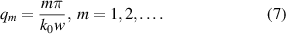
We have recently compared various approaches to numerical modelling of light propagation in a silicon waveguide with graphene overlay [22], and we revealed quite irregular fluctuations of both attenuation and phase of the guided mode in dependence of the chemical potential above approximately 0.5 eV. At first, this effect appeared to be a numerical artifact of the simulation method used, however it was reproduced also in other, completely independent simulation approaches, and it was reported in [23]—see figure 1. Since we were interested in the mechanism behind this effect, we decided to analyze it in more detail. In this communication, we show that this effect is due to the coupling of surface plasmon modes supported by the graphene stripe ('ribbon plasmons' [24]), even at the telecommunication optical wavelength band around 1550 nm, with the mode of the silicon waveguide. To demonstrate this, we calculate the complex propagation constant of the (quasi-) TE mode of the silicon waveguide loaded with the graphene stripe using a strongly simplified coupled mode theory (CMT) and compare it with a full-wave numerical simulation using the commercial software packet COMSOL Multiphysics [25]. We show that despite the rather crude simplifications used in our implementation of the CMT, the similarity of both results is convincing.

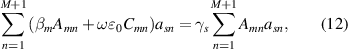
Figure 1. Rib silicon waveguide with graphene layer.
Download figure:
Standard image High-resolution imageA simplified structure of the Si rib waveguide modulator with a graphene layer used for the comparison, inspired by the design described in [7], is shown in figure 1.
The geometrical parameters of the waveguide structure analyzed here are close to those used in practical devices: the total silicon layer thickness is  the rib waveguide width is
  , the residual silicon thickness after the shallow etch is
  The graphene layer is deposited only on the top of the rib waveguide, separated from silicon with a thin SiO2 layer,
  The superstrate is air. The wavelength of the optical wave propagating in the waveguide is
The paper is organized as follows: in the next section, we review the properties of surface plasmons at the vacuum optical wavelength of 1550 nm supported by a graphene layer, and present an approximate solution of plasmonic modes propagating along the graphene stripe. Then we describe a simplified coupled-mode theory for the coupling of the multitude of graphene plasmonic modes with the mode of the silicon waveguide and confirm the qualitative CMT results with a 'rigorous' full-wave numerical electromagnetic solution obtained with COMSOL Multiphysics [25]. In the final section, we discuss the effect of coupling of the surface plasmons with the waveguide mode on the physical properties of the waveguide structure that may be useful in design and operation of silicon photonic devices with graphene layers.
2. Surface plasmons on graphene
Although the properties of surface plasmons supported by a graphene layer have already been analyzed in detail [24, 26–28], most publications concentrate on the mid-infrared spectral region. We thus first review the properties of surface plasmons at the telecom wavelength band of 1550 nm propagating along the graphene sheet sandwiched between two dielectric media—in this case SiO2 and air. The optical properties of a graphene monolayer are determined by its complex surface conductivity  , which can be described with an approximate expression [1, 27] (note that we use the convention
  for time-harmonic quantities):
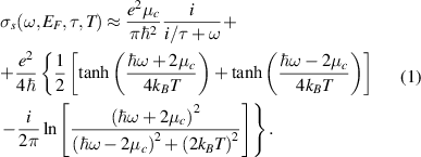
Here,  are the circular frequency of light, the chemical potential of the graphene layer, the time constant corresponding to the graphene relaxation time, the absolute temperature, the Boltzmann constant and the reduced Planck constant, respectively. We used the following values in our simulations:
  (corresponding to the optical free-space wavelength of 1550 nm),
  and
and  The dependences of the real and imaginary parts of the surface conductivity on the chemical potential, calculated from (1) for
  are shown in figure 2. Note that in the range of
  the positive imaginary part of the surface conductivity strongly prevails.

Figure 2. Real and imaginary parts of the surface conductivity of graphene σs at λ = 1550 nm in dependence of the chemical potential μc.
Download figure:
Standard image High-resolution imageThis is a condition allowing propagation of a surface plasmon at the interfaces of a graphene layer, considered as an infinitely thin layer with a finite surface conductivity  , sandwiched between two dielectrics.
2.1. Surface plasmon on an infinite graphene sheet
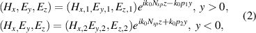
For further considerations, we need to know the surface plasmon propagation constant and field distribution in dependence of the chemical potential of the graphene layer with parameters given above. Let us first consider propagation of a (TM polarized) surface plasmon in the z direction on a planar structure unlimited in the  direction (the coordinates axes are considered as in figure 1). Such a wave has a single magnetic field intensity component
  and two electric field intensity components
  . Their field distributions in dielectric media are
where  is the (complex) effective refractive index of the surface plasmon, also called a modal index [29],
  is the propagation constant,
  and
and  are the (normalized complex) transverse decay constants into air and SiO2 substrate, respectively, and
  is the vacuum wavenumber.
Next, it follows from Maxwell equations that
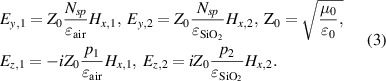
The field continuity conditions at the graphene layer sound as

The dispersion equation for the surface plasmon is then obtained from (3) and (4) in the form
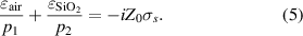
Realizing that  , this equation can be cast into the fourth-degree polynomial in the variable
  . However, not all roots of this polynomial also satisfy the original dispersion equation (5). Moreover, according to (2), the existence of the surface plasmon as a physically realizable wave confined to the graphene layer and decaying in the direction of propagation requires that the real parts of both
  and
and  and the imaginary part of the effective refractive index
  are positive. At the wavelength of 1550 nm, just one surface plasmon wave is supported in our structure in the range of the chemical potential
  considered in figures 3 and 4. These figures show real and imaginary parts of the effective refractive index of the surface plasmon, its propagation length
 ![${L_{sp}} = 1/\left[ {2{k_0}Im\{ {N_{sp}}\} } \right]$](https://content.cld.iop.org/journals/2040-8986/22/9/095801/revision2/joptaba965ieqn31.gif) , and its penetration depths into air and SiO2,
, and its penetration depths into air and SiO2,  and
and  , respectively.

Figure 3. Real and imaginary parts of the effective refractive index Nsp of the surface plasmon in dependence of the chemical potential μc for the free-space wavelength of 1550 nm.
Download figure:
Standard image High-resolution image
Figure 4. Propagation length  and penetration depths
  and
and  of the surface plasmon in dependence of the chemical potential
  for the free-space wavelength of 1550 nm.
Download figure:
Standard image High-resolution imageNote that in the range of  the propagation length typically reaches a fraction of a micrometer, and the penetration depths into both dielectric media are practically the same, of the order of a few nanometers, due to the very large effective index of the plasmon mode,
  From this approximation and (3), it also follows that electric field intensity components are practically equal in magnitude, although mismatched in phase,
  , and magnetic field components are scaled with respect to the permittivities of the surrounding media,
  A very strong vertical confinement of the surface plasmon justifies the fact that the proximity of silicon was neglected in this analysis. Its influence will be taken into account later in the CMT approach.
2.2. Surface plasmons on a graphene stripe
The surface plasmon mode propagating in the z direction, described in the previous section, cannot couple with the guided mode of the silicon waveguide because of a huge (1–2 orders of magnitude) mismatch of their effective refractive indices (note that the effective refractive index of the quasi-TE mode of the silicon waveguide at  calculated with COMSOL is 2.3754). However, the graphene stripe on top of the silicon ridge waveguide in figure 1 supports a number of higher order ('nanoribbon' [24, 30–32]) modes with smaller propagation constants, and some of them can match with that of the mode of the silicon waveguide. We will use the approach of the effective-index method (EIM) [33] to approximately determine their propagation constants and field distributions. Similarly to a mode of a planar dielectric waveguide, the plasmonic modes of a graphene stripe result from the interference of two plasmons that are propagating under some angle with respect to the z axis and are reflecting from the stripe edges. Following the idea of the EIM, the dispersion equation for such modes can be written in the form of the transverse resonance condition (in the x direction)

where  is the transverse propagation constant of the mth mode,
  is the mode number, and
  is the (amplitude) reflection coefficient of the plasmon from the edge of the graphene stripe.
Reflection and scattering of a surface plasmon from discontinuities in the graphene plane–including the reflection from the edge of a graphene stripe–has already been studied in detail and reported in a number of recent papers [31, 34–39]. It has been found that the reflection at the stripe edge is close to the total,  while the phase of the reflection coefficient nontrivially depends on the detailed morphology of the graphene edge, on the inhomogeneity of the graphene conductivity due to redistribution of charges, on the excitation of evanescent waves near the stripe edge, etc. To keep our analysis as simple as possible, we decided not to consider this anomalous phase shift. Numerical tests with various kinds of boundary conditions (perfectly electric or magnetic (PMC) walls and Fresnel reflection coefficients) finally led us to the application of the PMC approach. This choice allows for a very simple evaluation of the effective refractive indices and the electromagnetic field distributions of the graphene stripe modes, which are quite close to those obtained by using more rigorous COMSOL simulations. Some lowest-order modes of the graphene stripe (including central and edge 'ribbon plasmons' [32]) are out of scope of this approach. However, these modes cannot couple with the mode of a silicon waveguide due to strong mismatch of their propagation constants.
By taking  , we obtain the solution of the dispersion equation (6) in the form
The effective refractive indices of the stripe plasmon modes are then obtained from the relation
In our approximation,  are real numbers. Since
  is complex, the effective refractive indices
  are complex too. Consequently, there is no clear transition between propagating and evanescent plasmonic modes of the graphene stripe. However, since the imaginary part of
  is significantly smaller than its real part, the real parts of high-order modes
  reach low enough values for efficient coupling with the fundamental (quasi-)TE silicon waveguide mode. However, their imaginary parts are nonzero, which indicates that the coupling may introduce a rather significant loss. As an example, the real and imaginary parts of the effective refractive indices
  of the graphene stripe are plotted in figure 5 for two values of the chemical potential,

Figure 5. Calculated real and imaginary parts of the effective refractive indices of the stripe plasmons as a function of the mode number for two values of a chemical potential,  The inset shows the detail of the transition from propagating to evanescent modes for
Download figure:
Standard image High-resolution imageA full-vector field distribution of plasmon stripe modes is given by the superposition of two surface plasmons with equal amplitudes and with the wave vectors  where the sign
  relates to the direction of propagation in the
  plane, and the subscripts
  are related to the regions
  and
and  respectively, in accordance with (2). Note that all components of electric and magnetic fields are nonzero, except for
  . Basics of the CMT describing simultaneous coupling of the mode of the silicon waveguide with several plasmon modes of the graphene stripe are briefly described in the next session.
3. Coupling of waveguide mode with surface plasmons on graphene stripe
Simultaneous coupling of a mode of a silicon waveguide with several plasmonic modes of a graphene stripe on top of the silicon waveguide can be considered as mutual coupling among modes of several parallel waveguides. One of the waveguides is the silicon waveguide, while the other 'waveguides' correspond to individual plasmonic modes supported by the graphene stripe. We denote the field distribution of the eigenmode of the silicon waveguide without graphene as

where  is its propagation constant. Similarly, the field distributions of plasmonic modes are
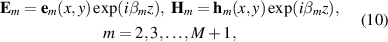
where  is the number of plasmonic modes taken into account. In this approach, the eigenmodes ('supermodes') of the complete waveguide system with the (generally complex and anisotropic) permittivity distribution
  are constructed as linear superpositions of eigenmodes of individual waveguides with the corresponding permittivity distributions
  ,
,
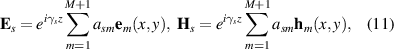
where  are the propagation constants and
  are the expansion coefficients of the 'supermodes'. Specifically,
  is the complete permittivity distribution of the waveguide structure including graphene layer as shown in figure 1,
  is the permittivity distribution of the silicon waveguide in figure 1 without the graphene layer, and
  are identical permittivity distributions containing the graphene stripe on the SiO2 pedestal of the width
  , surrounded by air. Applying the principles of the complex CMT [40, 41] (chapter 10), we arrive to the following generalized eigenvalue equation for the complex amplitudes
  and the propagation constants
  :
:
where
Here,  denotes the electric field distribution of the mth mode with inverted z-component, and S is the cross-section of the whole waveguide structure. Using similar arguments as in [22], we obtain
In our simplified implementation of the CMT, we further neglect off-diagonal elements of the matrix A, ignore mutual coupling among various graphene modes, i.e. we set  for
for  and
and  , and assume that
  , where
  is given by equation (14). Such a procedure helps significantly simplify the calculation, while keeping all aspects important for our analysis: the diagonal terms of the matrix C represent corrections to the propagation constants of modes due to modified waveguide structure and thus affect the phase mismatch among the interacting modes, while the off-diagonal elements of C describe the coupling of the silicon waveguide mode with plasmonic modes of the graphene stripe. Note that if we retain only the first terms
  and
and  in (12), i.e. if we neglect the coupling, we obtain for the propagation constant
  an expression equivalent to that obtained with the perturbation method in [22], equation (10).
The variance of real and imaginary parts of the effective refractive index of the (quasi-)TE mode of the silicon waveguide due to the presence of the graphene layer is shown in figure 6 in dependence of its chemical potential. The results of three methods are presented there. The red line corresponds to the results of the perturbation method of [22] that does not take into account the coupling with the surface plasmon modes in the graphene stripe, the blue line represents the result of a numerical simulation with COMSOL, and the yellow line shows the CMT results. In the COMSOL simulations, the graphene layer was represented by a boundary condition with surface conductivity [22]. The results obtained by using COMSOL and our approximate CMT method are in fairly good agreement and provide convincing physical arguments for the presence of coupling between TE polarized silicon waveguide modes and graphene surface plasmon modes.

Figure 6. The variance of (a) real and (b) imaginary parts of the effective refractive index of the TE mode of the silicon rib waveguide due to graphene stripe as a function of the graphene chemical potential. Blue line: numerical solution using COMSOL, red line: perturbation method (PT), yellow line: coupled mode theory (CMT). Interval of  from 1.4 to 2 eV in figure 6(a) is zoomed in the inset for better resolution.
Download figure:
Standard image High-resolution imageThe graphs in figure 6 show that the coupling of the silicon waveguide mode with surface plasmon modes of the graphene stripe has a typical resonant character. When the chemical potential is gradually changing (due to chemical doping or applied external electric field), the propagation constant  of the surface plasmon on the graphene sheet is changing too, as is shown in figure 3. Consequently, the propagation constants
  of plasmonic modes of the graphene stripe are gradually changing too. Just one of them in a time comes into resonance with the propagation constant of the silicon waveguide, and both the phase and amplitude of the waveguide mode are affected by the coupling. For
  the peaks of the imaginary part of the effective index of refraction of the silicon waveguide mode caused by coupling with graphene stripe plasmon modes are of the order of
  , which corresponds to a rather strong attenuation of the silicon waveguide of the order of several dB/mm.
Figure 7 shows the distribution of the horizontal electric field intensity component of the fundamental TE mode of the silicon rib waveguide coupled with a surface plasmon on the graphene stripe, calculated with COMSOL, for the resonance value of  (see figure 6). The 'decoration' of the mode field with the field distribution of the surface plasmon is apparent. Note that, according to (13), only surface plasmon modes with the same symmetry can couple with the silicon waveguide mode.

Figure 7. (a) Distribution of the  component of the fundamental TE mode of the silicon waveguide coupled with the surface plasmons of the graphene stripe. The chemical potential of graphene is 1.61 eV. (b) Zoom of the
  field distribution of the graphene stripe plasmon on the top of the silicon waveguide mode.
Download figure:
Standard image High-resolution image
Although the dominant electric field component of the plasmons is vertical  , there is curiously negligible coupling among the graphene plasmons and the TM-polarized waveguide mode. The reason stems from the nature of the coupling mechanism. According to (13), only electric field components parallel with the graphene layer can contribute to the coupling; apparently, there is no graphene conductivity in the vertical direction. When a graphene layer is also deposited on the side walls of the silicon waveguide (as was considered, e.g. in [22]), graphene stripe plasmon modes supported by the side walls can contribute to the coupling too. As a result, the (quasi-)TM waveguide mode is also affected, the graphene mode spectrum is more complicated, and so are the phase and attenuation dependences of the waveguide mode on the chemical potential of the graphene layer.
4. Conclusions
Propagation of surface plasmons on graphene sheets has been previously studied, mostly in the THz and infrared frequency ranges. On the other hand, graphene layers on silicon waveguides have recently been used very often in the design and construction of photonic devices for modulation, switching, etc. These devices typically operate within the telecommunication band around 1550 nm, where the surface plasmon propagation on graphene layers has attracted much less attention. In this communication, we show that in the range of the chemical potential of graphene above 0.5 eV, surface plasmons supported by graphene stripes deposited on the top of a silicon waveguides rather strongly affect their guiding properties due to the coupling of surface plasmons with the mode propagating in the waveguide. This effect has been independently studied by both the approximate method based on the CMT, and by 'rigorous' numerical simulations using COMSOL. Although the accuracy of the approximate method is not high, it offers a deep insight into the process and contributes to the understanding of the details of the coupling mechanism. The effect has not necessarily been considered harmful for the operation of silicon photonic devices, rather it may be employed in design of specific devices such as low-power modulators and sensors. Although our analysis was focused at the near infrared telecom wavelength range, we are highly convinced that this effect takes place not only in the near- to mid-IR silicon transparency window, but also in the THz spectral range where the silicon waveguides are being used as well [18, 42–44].
Acknowledgments
This work was financially supported by the Czech Science Foundation under Project 1900062S and by the Project Center of Advanced Applied Sciences CZ.02.1.01/0.0/0.0/16_019/0000778—European Structural and Investments Funds—Operational Programme Research, Development, and Education.