

Abstract
Nanopillars of ZnO were implanted with Au-400 keV ions at various ion fluences from 1 × 1015 cm−2 to 1 × 1016 cm−2 and subsequently annealed at 750 °C for 15 min in order to reduce the implantation damage and to support Au nanoparticle (NP) aggregation. It was found that implantation-induced effects and thermal effects influence the Au NP coalescence as well as the quality of the ZnO nanopillars. Rutherford Back-Scattering spectrometry (RBS) showed the broader Au-depth profiles than it was theoretically predicted, but the Au-concentration maximum agrees well with prediction taking into account the effective ZnO layer density. The implantation at the higher fluences induced the morphology modification of the nanopillar layer evidenced by RBS and scanning electron microscopy (SEM). An indirect evidence of this effect was given by optical ellipsometry due to gradual refractive index changes in the ZnO nanopillars with the increased Au-ion fluence. Optical characterization of the Au-implanted and annealed nanopillars performed by means of photoluminescence (PL) and diffuse-reflectance spectroscopy (DRS) evidenced the surface plasmon resonance (SPR) activity of the embedded Au NPs. The SPR-enhanced scattering and PL emission observed in the spectral range 500–650 nm are ascribed to Au NPs or more complex Au-clusters. In addition, the ellipsometry measurements of extinction coefficient are found to corroborate well results from DRS, both indicating increase of SPR effect with the increase of Au-ion fluence and after the post-annealing.
Export citation and abstract BibTeX RIS
1. Introduction
We present our recent results obtained in Au-ion implantation of ZnO nanopillars for Au nanoparticle (NP) creation. Ion implantation is a versatile technique that makes it possible, by adjusting the implantation ion energy and fluence, to modify the electrical, mechanical and optical properties of bulk and nanostructured materials [1, 2], as well as to introduce micro- and nano-structures via energetic heavy ions. ZnO reportedly has an extraordinarily high radiation tolerance in comparison to other semiconducting materials such as GaN or GaAs [3]. Moreover, a unique set of material properties such as wide band gap (3.37 eV), large free-exciton energy (60 meV) and high luminescence efficiency [4, 5] together with feasibility of nanostructuring make ZnO very attractive for the fabrication of nano-optics devices, as well as for DNA sensor and biological applications in general [6–8]. Au-metal NPs can expand the light absorption range of ZnO and can greatly enhance the ZnO photocatalytic activity given their plasmonic or luminescence properties. Metal oxides such as ZnO are nowadays being investigated as efficient photocatalysts and antimicrobials agents [9]. The optical activity of metal NPs is strongly affected by their shape, size, geometrical configuration, structure and composition. Ion implantation and irradiation are unique tools for the synthesis and modification of NPs in various host matrices and semiconductors as well. Since implanted noble metal-ions have larger radii than Zn, they tend to coalesce while inducing a dense collision cascade, which strongly modifies the ZnO wurtzite host matrix [10, 11]. Semiconductor nanocrystallites with a dopant can exhibit unique optical and electronic properties [12, 13], mainly in the case of Au [14]. Presently, the research focus is gradually shifting towards the formation of radiation defects in ZnO, where significant connections between the dopant's chemical nature and defect formation have been revealed [3, 10, 11, 15, 16]. Damage accumulation, dopant positioning and defect‒dopant interaction influencing defect stabilisation in bulk ZnO etc, are all crucial issues for the understanding of the complex processes taking place in ion beam irradiated ZnO nanopillars.
Nowadays, ZnO thin films and nanostructures can be synthesised by using various deposition techniques, such as molecular beam epitaxy [17, 18], metal‒organic chemical vapour deposition (CVD) [18, 19] etc. ZnO possesses a large variety of nanostructures whose optical properties have been very intensively investigated [20]. Owing to its highly anisotropic wurtzite structure, vertically aligned ZnO nanowires can be formed as building blocks in a wide variety of applications [21, 22].
Post-implantation annealing is typically used to restore the crystalline structure and also to improve the optical properties [23]. It should be noted that the removal of point defects is already observed at temperatures below 500 °C in single crystalline ZnO due to strong annealing of uncorrelated defect structures such as point defects and small defect clusters [24]. A complete removal of ion-induced extended defects in single crystalline ZnO typically requires relatively high temperatures exceeding 900 °C‒1000 °C, as reported for other ion species including Ag in [25, 26]. Furthermore, the implanted atoms themselves can stabilise radiation defects, while pronounced loss or out-diffusion of implanted atoms may lead to efficient recovery of the crystalline lattice and coalescence of the introduced dopant.
The situation differs in ZnO nanostructures, where radiation defects in the ion-implanted nanopillars can be successfully recovered using rapid thermal annealing in oxygen at lower temperatures between 700 °C and 950 °C. Sufficient annealing has to be performed in order to remove the implantation defects; short duration and low enough temperature annealing is desirable in order not to degrade the implanted ZnO nanorods [27]. Moreover, moderate annealing is necessary to avoid deactivating the dopants [27]. It was observed in [28] that temperatures from 700 °C to 900 °C for 15 min can recover the outer shell of the ZnO nanowire from 35 to 70 nm thick, respectively. However, at the higher temperature, the nanowire exhibits rough side facets instead of the perfectly flat ones for as-grown samples. The surface degradation has been ascribed to annealing-induced surface degradation of the implanted ZnO nanowires in [28] and a thermal deterioration effect was confirmed also in high As-ion fluence implanted nanorods after annealing at 950 °C–1000 °C in [29].
It was demonstrated that the dislocation elimination in ZnO nanowires is facilitated by the nanowire free surfaces, allowing shorter duration annealing at lower temperatures [29], and increasing the time of annealing above 20 min can be detrimental rather than beneficial. Au NP coalescence in materials such as sapphire after Au implantation can be achieved already at temperatures of about 600 °C [30], but typically longer annealing times are chosen to cause the coalescence of particles bigger than 10 nm. The photoluminescence (PL) of doped ZnO nanobelts has been nearly fully recovered after annealing at 800 °C, with 15 min under vacuum in [31]. Optical properties can be modified differently due to distinct radiation damage accumulation in various crystallographic orientations of ZnO [32]. The different radiation damage can play complex role in case of ZnO nanopillars with many facets facing the ion implantation beam. The PL spectra have revealed that the near band edge (NBE) gap exciton-related luminescence band of Au:ZnO bulk samples was partially restored for all crystal planes after thermal annealing at 600 °C due to the recovery of the ZnO structure. After the annealing, the NBE band was restored with the highest intensity in the c-plane [32].
Our experiments were motivated by the following issues: (a) the structural damage in ZnO nanopillars after the Au-ion implantation and its recovery after the annealing, (b) Au incorporation and NP formation in ZnO nanopillars, (c) optical and luminescence properties of ion beam modified ZnO nanopillars.
2. Experiment
2.1. Structure analysis of Au-implanted ZnO nanopillars by x-ray diffraction (XRD), Rutherford back-scattering spectrometry (RBS) and scanning electron microscopy (SEM)
ZnO nanopillars were grown on Si wafers using a hydrothermal approach [33]. Polished silicon wafers 1 × 1 cm in size from Siegert Wafer (Germany) with the orientation of <100> ± 5° were immersed for 10 min in a 75 °C solution of deionised H2O (0.055 μS cm−1, Evoqua, USA), NH3 (30%, Chemsolute, Germany), H2O2 (25%, Chemsolute, Germany) in the ratios of 5:1:1, followed by rinsing in deionised H2O and a further cleaning two times in an ultrasonic bath. Afterwards, they were dipped for 20 s in a solution of 0.005 mol l−1 zinc acetate (Alfa Aesar, UK) in isopropanol (Chemsolute, Germany) and rinsed immediately with isopropanol. This procedure was repeated four times to assure a continuous coverage of zinc acetate. The samples were heated for 20 min at 350 °C to get a thin layer of calcined ZnO seeds on the silicon substrate. The samples were placed almost vertically in 50 ml tubes, with the top side facing slightly downwards. An equimolar solution of 0.05 mol l−1 zinc nitrate (Alfa Aesar, UK) and hexamethylenetetramine (Alfa Aesar, UK) in deionised H2O was filled in the tubes and used as deposition solution. Finally, the samples were cleaned five times in an ultrasonic bath with deionised H2O. ZnO nanopillars were implanted with the Au-400 keV ions using the fluences of 1 × 1015 cm−2, 5 × 1015 cm−2 and 1 × 1016 cm−2 using an implantor at the Ion Beam Center, HZDR Dresden-Rossendorf, Germany. The implanted samples were subsequently annealed at ambient atmosphere at 750 °C for 15 min in a conventional furnace in order to reduce the implantation damage and to support Au NP aggregation.
2.2. Structure analysis of ZnO nanopillars with implanted Au by XRD, RBS and SEM
XRD was utilised for the study of the crystal-structure modification of the pristine ZnO nanopillars as well as those with Au NPs. We used a Rigaku SMARTLAB 9 kW rotating-anode generator and CuKα1 characteristic radiation; the diffractometer was equipped with a primary parabolic multi-layered mirror and a 2 × 220 Ge channel-cut monochromator. In the middle-resolution (MR) set-up we used a linear detector on the secondary side, while for high resolution (HR) we applied a secondary 2 × 220 Ge channel-cut analyser and a point detector. The MR set-up was used for long-range 2Θ-scans keeping the incidence angle constant ( ). Almost symmetric 2Θ/ω scans were measured in the HR set-up; in these scans we avoided very intense diffraction peaks of the Si substrate by introducing the angular offset of
RBS was employed for characterisation of ZnO nanopillars using a beam of 2.0 MeV He+ ions from a Tandetron accelerator using the detector placed at scattering angle 170°. Simultaneously, RBS was used for the implanted Au depth profile analysis.
SEM was realised using a TESCAN MAIA 3 instrument with a field emission gun (TESCAN, Czech Republic). All samples were attached to SEM stubs using double-sided conductive carbon tape. For side-view imaging, a small piece of Si substrate was cleaved to expose the transition between the substrate and ZnO nanopillars. For all samples, imaging was performed in high vacuum at 5 kV accelerating voltage using an in-beam detector.
2.3. Optical characterization by ellipsometry, diffuse-reflectance and PL spectroscopy
The optical emission properties of ZnO nanopillars were investigated by PL measurements carried out at 10 K by employing a closed-cycle He refrigerator system and using a 325 nm wavelength He–Cd laser as an excitation source (power density ∼20 W cm2). The PL spectra were recorded by fiber-optic spectrometers (Ocean Optics HR4000/USB4000) with a spectral resolution below 2 nm. The optical scattering and absorption properties were investigated at room temperature by means of diffuse-reflectance spectroscopy (DRS) using EVO-600 (Thermo Fisher Scientific, Inc.) UV–Vis spectrophotometer.
The spectra of the ellipsometric parameters were recorded by a VASE ellipsometer (JA Woollam Co.) in the VIS spectral range for incidence angles of 50°‒80°. Reflectance measurements were carried out by the same instrument and were numerically treated simultaneously along with the ellipsometry with the help of WVASE commercial software. In the investigated spectral range, the light beam reflected from ZnO nanopillars showed predominantly specular reflection with a negligible diffused component. Ellipsometric spectroscopy, as an indirect characterisation technique, requires a sample model and materials optical constants in the form of table data or parameterised dielectric functions. The sample model consisted of crystalline Si substrate with a SiO2 native oxide over-layer (2.5 nm) covered by ZnO nanopillars. The ZnO nanopillar layer was modelled as a layer with a gradient profile of refractive index. The non-uniform thickness of the ZnO nanopillar layer was also accounted for and was found to be closely related to the recorded depolarisation factor. The optical constants of crystalline Si were taken from the WVASE software database. The ZnO optical constants were parameterised by Cauchy dispersion relation extended with the short-wavelength exponential absorption edge [34]. The upper (surface) part of the ZnO layer, where the implantation of Au ions was expected, was further described by an additional Lorentz harmonic oscillator to account for possible Au local surface plasmon resonance (SPR) (see supplementary material for details available online at stacks.iop.org/JPhysD/55/215101/mmedia).
3. Results
3.1. Theoretical SRIM simulations of Au-ion interaction with ZnO
For a better understanding of the electronic and nuclear stopping interplay in the implanted ZnO, SRIM calculation [35] of energy stopping was performed. Additionally, we calculated the projected range using SRIM for the Au-400 keV ions as RP = 65 nm with the standard deviation ΔRP = 19 nm. SRIM calculation of the Au-ion 400 keV depth profiles, O and Zn vacancies creation (displacement energies for Zn and O used in SRIM calculations were referred to in [15, 16]) and the energy stopping in ZnO nanopillars has been provided. However, it must be emphasised that SRIM calculation is not capable of taking into account any morphological aspects, so a 500 nm thick ZnO bulk layer with ZnO bulk density is taken into account in the calculation in figures 1(a) and (b). Moreover, we provided additional simulation with the effective density calculated by using the known ZnO nanopillar layer thickness as it was determined from SEM cross-section measurement on the pristine samples (see section 3.3). The projected height of the ZnO nanopillars was averaged over several SEM measurements being about 380 nm (taken as a perpendicular thickness of the nanopillar layer facing the penetrating ion implantation beam). Additionally, based on the RBS analysis, the pristine sample exhibited an areal atomic density of the ZnO nanopilar layer 1626 × 1015 atoms cm−2 taking into account Zn and O atoms (see section 3.2, table 1).
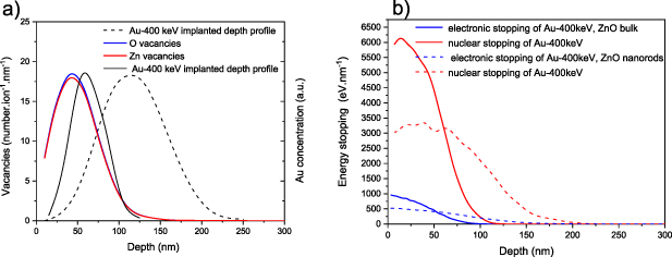
Figure 1. SRIM calculation of energy stopping of the Au-ions used in ZnO nanopillar implantation: Au-400 keV ion depth distribution and O, Zn vacancy depth profiles in (a) and energy stopping in (b), respectively. The solid lines represent the SRIM calculation with ZnO bulk density (5.61 g cm−3) and the dashed lines represent the SRIM calculation with the effective density of the ZnO layer with nanopillars (3.0 g cm−3).
Download figure:
Standard image High-resolution imageTable 1. Summary of RBS results presents the Au integral amount, the ZnO layer thicknesses in atoms cm−2 for the implanted and sub-sequently annealed ZnO nanopillars at various Au-ion implantation fluences.
| Sample/Au-ion fluence/annealing | Au integral amount (1015 atoms cm−2) | ZnO layer thickness (1015 atoms cm−2) |
|---|---|---|
| ZnO/1 × 1015 | 1.2 ± 0.3 | 1600 ± 200 |
| ZnO/5 × 1015 | 4.3 ± 0.3 | 1100 ± 200 |
| ZnO/1 × 1016 | 9.4 ± 0.3 | 1200 ± 200 |
| Pristine | 0 | 1600 ± 200 |
| ZnO/1 × 1015/annealed | 1.1 ± 0.3 | 1600 ± 200 |
| ZnO/5 × 1015/annealed | 4.5 ± 0.3 | 1100 ± 200 |
| ZnO/1 × 1016/annealed | 9.3 ± 0.3 | 1200 ± 200 |
The known areal atomic density of the ZnO layer and the independently determined average ZnO layer thickness from SEM analysis were used to determine the effective density of ZnO nanopillar layer (3.0 g cm−3) differing significantly from the density of bulk ZnO (5.61 g cm−3). SRIM calculation of the Au-400 keV projected ranges with the modified ZnO layer density is presented for comparison in figure 1(a) (dashed line) and electronic and nuclear stopping powers are shown in figure 1(b) (dashed lines). It is clear, that ZnO nanopillars would suffer with higher uncertainty of the Au-ion projected ranges due to significant ion-energy straggling during the penetration through voids in ZnO layer. The projected range and standard deviation for the ZnO layer with the effective density 3.0 g cm−3 was calculated by SRIM as RP = 120 nm, ΔRP = 36 nm.
3.2. Elemental and structural analysis by RBS and XRD
The results published recently in [16, 32, 36] give us a picture of the distinct radiation damage growth, Au NP coalescence and optical response in ZnO single crystalline orientations, which should be taken into account in the case of the experiment with ZnO nanopillars implanted by Au-400 keV ions. Au NP coalescence in such ZnO nanopillars and their resulting optical response might differ from ZnO bulk as radiation damage, accumulated in polar and non-polar planes, taking place at the same time and radiation defects would cumulate distinctly due to the high effective ZnO surface acting as a sink for defects.
RBS analysis was used to follow, at least qualitatively, the Au distribution in ZnO nanopillar layer. The pristine ZnO nanopillars were not fully oriented along c-axis <0001>, so structural analysis based on the ion channelling effect is not possible. Moreover, the depth scale calculation is strongly affected by the complex morphology and high roughness of ZnO nanopillar layer. Besides, the density cannot be taken as the bulk ZnO density.
However, we can qualitatively follow the RBS spectra of ZnO nanopillars deposited on Si, where we saw the modification of the Zn and O signals from the ZnO nanopillars layer. The spectra of the pristine and the as-implanted ZnO nanopillars are presented in figure 2(a). The Au depth profiles are presented in figure 2(b). In general, the Au depth profiles measured by RBS differ from the SRIM simulation for bulk ZnO layer (with the bulk density 5.61 g cm−3). RBS profiles are broader and exhibit an asymmetric Au-distribution. Implantation into the nanopillars differ from implantation into compact layers and suffered from a strong scattering of the projected ranges of the implanted ions, so that the Au ion distribution was much broader than it was theoretically calculated. However, it can be suggested that the Au coalescence can take a place within the major part of the nanopillars. RBS did not evidence Au content in the Si substrate.

Figure 2. RBS spectra of the pristine, as-implanted and as-annealed ZnO nanopillars implanted with 400 keV Au+ ions using various fluences in (a) and Au concentration depth profiles in Au-implanted ZnO nanopillars in (b).
Download figure:
Standard image High-resolution imageAdditionally, RBS analysis is sensitive to a surface morphology, where a high roughness and porosity of the ZnO surface can be mimicked by the typical in-depth tales at Au-depth profiles. A roughness effect exhibited in the RBS depth profiles can be simulated properly in case of the surfaces with regular and simple morphology, as it was investigated e.g. in [37, 38]. We can conclude that RBS analysis determined the depth of the Au maximal concentration. However, the in-depth tail of the Au-peak in the RBS spectra (see figure 2(a)) could be connected to the surface roughness effects [37, 38]. The effective density of the ZnO layer was used for converting the depth scale of the Au-depth profile evaluation to nm.
We observed the Au-concentration maximum shift to the surface in the ZnO nanopillar layer with increasing Au-ion fluence in the implanted samples (see figure 2(b)). It can be connected to the deterioration of the ZnO nanopillar layer in the upper part facing to the ion implantation beam.
We performed the detailed analysis of the ZnO thicknesses in atoms cm−2 from RBS spectra showing the total number of Zn and O atoms in the layer. The results are summarized in table 1. The ZnO thicknesses in atoms cm−2 decreased for fluences of 5 × 10¹⁵ and 1 × 1016 cm−2. It showed us ZnO nanopillar layer degradation under the Au-ion bombardment. Zn depletion in RBS spectra can be connected to nanopillar erosion as it was observed also in [39] after Cu-ion implantation of ZnO nanorods. ZnO surface morphology modification can cause the Zn-signal asymmetry in the RBS spectrum [38, 39].
This effect could be related also to the compaction of ZnO nanopillars layer at the bottom part, while sputtering effects would degrade the ZnO nanopillar upper parts. The annealing slightly influenced the Au depth profile shapes (see figure 2(b)) without a clear correlation to the Au-ion fluence, however the Au-integral amount did not change (see table 1). We did not see significant changes of the Zn peak in the RBS spectra of the annealed samples compared to the implanted samples (see table 1 showing ZnO thicknesses after the annealing); thus, the annealing modifies the internal structure rather than the ZnO nanopillar layer thickness.
XRD analysis of ZnO nanopillars was carried out by combining the MR 2Θ scans with the HR 2Θ/ω scans. The former experiments yielded much higher diffracted intensity, which made it possible to determine the ZnO lattice parameters from a large number of diffraction maxima with sufficient accuracy. Moreover, these measurements are suitable for searching for possible (very weak) diffraction peaks of possible Au NPs. On the other hand, the high diffracted intensity of the 2Θ scans is achieved by a much worse angular resolution, so that these scans cannot be used for the determination of the size of the coherent domains in nanopillars.
Figure 3 displays the 2Θ scans measured before (blue) and after (red) annealing. All the ZnO diffraction maxima could be identified in the measured curves. Most probably, additional non-identified peaks (denoted by question marks in figure 3) correspond to long tails of diffraction maxima of the Si substrate (crystal truncation rods). These peaks very sensitively depend on the azimuthal sample orientation and this is the reason why they do not appear in all diffraction curves. The ZnO peak heights roughly correspond to the calculated intensities; therefore, the ZnO layer is polycrystalline with no strong texture. Au diffraction peaks were fully not resolved, only in the curve of the annealed sample implanted with the highest Au fluence (figure 3(d), the red curve) not fully resolved Au reflections 111 and 200 might be suspected.

Figure 3. Medium-resolution 2Θ scans measured before (blue) and after (red) annealing of the pristine sample (a) and samples implanted with fluences of 1015 cm−2 (b), 5 × 1015 cm−2 (c) and 1016 cm−2 (d). In panels (a)–(d) we also plotted the theoretical positions and heights of the diffraction maxima of ZnO (black) and Au (green). Most likely, the peaks denoted by red question marks correspond to the Si substrate diffraction maxima (see the main text for explanation).
Download figure:
Standard image High-resolution imageWe fitted the individual ZnO diffraction maxima to Voight functions and from the positions of the diffraction maxima we determined the ZnO lattice parameters (see table 2). For this procedure, we used the well-known Cohen‒Wagner approach modified for hexagonal crystals [40].
Table 2. The lattice parameters and radii of ellipsoidal coherent domains in ZnO nanopillars as implanted with Au-400 keV ions and as-annealed at the various ion-fluences are compared to the pristine ones.
| Au-ion fluence (ions−2) | ZnO nanopillars—as-implanted; lattice parameters (Å) | ZnO nanopillars—as-annealed; lattice parameters (Å) | ZnO nanopillars—as-implanted; domain radii (nm) | ZnO nanopillars—as-annealed; domain radii (nm) |
|---|---|---|---|---|
| Pristine | a = 3.244 ± 0.002 c = 5.198 ± 0.001 | a = 3.242 ± 0.002 c = 5.192 ± 0.001 |


|


|
| 1 × 10¹⁵ | a = 3.243 ± 0.002 c = 5.192 ± 0.001 | a = 3.241 ± 0.002 c = 5.189 ± 0.001 |


|


|
| 5 × 10¹⁵ | a = 3.241 ± 0.002 c = 5.196 ± 0.001 | a = 3.243 ± 0.002 c = 5.192 ± 0.001 |


|


|
| 1 × 10¹⁶ | a = 3.243 ± 0.002 c = 5.198 ± 0.001 | a = 3.245 ± 0.002 c = 5.194 ± 0.001 |


|


|
The HR offset scans are displayed in figure 4. From the integral widths  of the HR diffraction maxima, we determined the mean sizes of the coherent domains in the ZnO nanopillars. We assumed that the domains are uniaxial ellipsoids oriented along the [0001], where the mean radii along and across [0001] are denoted RB and RV, respectively. We reformulated the Williamson‒Hall approach [41] for ellipsoidal domains. The domain radii are determined from the minimum of the following residuum function.


Figure 4. HR offset scans of several diffraction maxima measured before (upper row) and after (bottom row) annealing and their fit by Voigt functions (lines). The parameters of the curves are the fluences in cm−2, P stands for the pristine sample.
Download figure:
Standard image High-resolution imagewhere the sum runs over individual diffraction peaks with diffraction angles  , the constant
  accounts for a possible microstrain in the nanopillars (assumed isotropic for simplicity), and:

Here we denoted  Å as the x-ray wavelength,
  is the shape factor, and
  is the angle between the ellipsoid axis (assumed to be parallel to [0001]) and the
  th diffraction vector. The resulting values of RB,V are summarised in table 2 as well.
Table 2 shows that the lattice parameters do not significantly change in the ZnO nanopillars after implantation or annealing. This indicated that Au dopant preferably would not enter any substitutional position, as was already seen in [42], but rather creates Au interstitials and clusters. However, we saw the modification in the basal and vertical domain radii decreasing with increasing Au-400 keV ion fluence. After the annealing, we observed the partial restoration of the domain sizes mainly in the basal direction and much less in the vertical direction. However, we can conclude from figure 3 that there is no full restoration of the diffraction peaks, keeping the broader FWHM and the lower intensity compared to the pristine sample. Thus the persisting damaged structure is evidenced in the ZnO nanopillars.
3.3. ZnO nanopillars morphology (SEM analysis)
Figure 5 shows the surface morphology and cross-sectional SEM images of the ZnO nanopillars grown on silicon substrates. Medium density and uniformly distributed nanopillars with the upper defined hexagonal facets were grown vertically on the substrates. However, some bending and not perpendicularly oriented nanopillars appeared in the pristine sample (see figure 5(a)). The diameters of the nanopillars were analysed from SEM images, being in the broad range from 77 to 139 nm and the thickness of the ZnO nanopillar layer was deduced from the cross-sectional images, being about 360‒400 nm. The morphologies of the nanopillars before and after the Au-400 keV ion implantation are presented with the ascending ion implantation fluence in figures 5(b)–(d), respectively.

Figure 5. SEM analysis of the surface and cross-section morphology of the pristine ZnO nanopillars and as-implanted with the Au-400 keV ions at fluences of 1 × 10¹⁵, 5 × 10¹⁵ and 1 × 1016 cm−2 in (a)–(d), respectively. The distance between bottom (Si substrate surface) and upper part of the ZnO nanopillar layer was measured as a perpendicular distance between indicated white lines from SEM cross-section images.
Download figure:
Standard image High-resolution imageWe observed degradation of the ZnO nanopillars in figure 5 for the higher Au-ion fluences as a result of radiation damage. This degradation is exhibited by sharpening of ZnO nanopillar tips, as well as interconnecting of the bottom ZnO nanopillar parts exhibited at the highest Au-ion implantation fluence (compare figures 5(a)–(d)). As the implantation fluence increased, the surface of ZnO nanopillars could be destroyed. Small pits were evidenced on ZnO nanorod surfaces implanted with Cu-ions by HR TEM in [39]. The authors suggested a pit aggregation into voids mainly after annealing. SEM images of the ZnO nanopillars after the annealing are presented in figure 6 for the higher Au-ion fluences of 5 ×10¹⁵ and 1 ×1016 cm−2 in figures 6(a) and (b), respectively. A very similar ZnO nanopillar morphology is observed after the annealing.

Figure 6. SEM analysis of the surface morphology of the ZnO nanopillars as-annealed after implantation with the 400 keV Au+ ions using implantation fluences of (a) 5 × 10¹⁵, annealed at 750 °C for 15 min and (b) 1 × 1016 cm−2, annealed at 750 °C for 15 min.
Download figure:
Standard image High-resolution image3.4. Optical properties of Au-implanted ZnO nanopillars
Optical emission and absorption properties of ZnO nanopillars addressed by PL and DRS techniques are summarized in figure 7. Note that these measurements were performed only on Au-implanted and annealed ZnO nanopillars along with the pristine (non-implanted) sample as a reference. The evolution of PL spectra obtained at 10 K as a function of Au-ion implantation fluence is shown in figure 7(a), where all curves are normalized with regard to the deep-level emission (DLE), the common feature dominating in all spectra. This way of presenting the data highlights the implantation-induced spectral changes within the broad DLE band, which is comprised of several partially overlapping and thus hardly distinguishable components. The original non-normalized DLE as well as the total luminescence yield appear as a rapidly decreasing function of implantation fluence (not shown), similarly to ion irradiated ZnO nanorods reported in [43].

Figure 7. Evolution of the optical emission and absorbance properties of ZnO nanopillars as a function of Au implantation fluence: (a) PL spectra measured at 10 K (data normalized in the DLE region). (b) Differential DRS obtained at 300 K. Shaded area highlights the common SPR region discussed in the text.
Download figure:
Standard image High-resolution imageThe pristine sample exhibits PL features typical to high-crystallinity ZnO—a narrow NBE peak at 368 nm (3.37 eV) associated with exciton recombination and a broad DLE band centered at around 600 nm (2 eV) originating from luminescent deep defect sites (VO—green luminescence, the transition between Zni and Oi levels—orange-red luminescence, etc) [32, 44]. By contrast, Au-implanted and post-annealed samples demonstrate generally suppressed NBE emission and apparent developments of DLE as function of the Au-ion fluence, particularly within the GL region centered at around 520 nm (2.4 eV). While the absence of NBE recovery after thermal annealing would be rather unusual for ZnO, in the present case of Au-implanted ZnO nanopillars this is accompanied with GL enhancement and thus might be indicative of an efficient charge transfer to plasmonic Au NPs. The similar effect of the charge transfer modification due to the increasing Au NP load in ZnO leading to NBE decrease and emerging of emission at 500 nm was observed in [45]. The spectral region of GL enhancement (highlighted by the shaded area in figure 7(a)) falls well within the reported PL activity range of Au NPs [46]. Indeed, SPR is a complex effect that modifies light coupling with a medium containing embedded Au NPs. The excitation of SPR in Au NPs results in an extreme concentration of light and an enhanced electric field around the nanostructures, leading to the significant enhancement in absorption and scattering efficiencies for photons at the resonant energy [47].
The light scattering phenomenon was addressed independently by means the DRS, where the detected signal, being directly proportional to the scattering efficiency, has provided a measure of SPR effect for different implantation fluencies. The differential DRS spectra presented in figure 7(b) are built by dividing each DRS by that of the pristine (non-implanted) ZnO nanopillars, and in this way directly exposing Au-implantation induced changes at different fluences. The well matching spectral regions of the enhanced scattering and GL emission in figures 7(a) and (b) strongly support their common plasmonic nature.
The absorption properties of ZnO nanopillars assessed by DRS indicate certain regions of the absorbance upturn (550–750)nm and downturn (450–600)nm with reference to the pristine (non-implanted) ZnO nanopillars (not shown). While DRS offers only qualitative assessments via Kubelka–Munk (K–M) function ascribed by both absorbance and scattering (sum of these parameters is extinction), the ellipsometry deals with extinction in a quantitative way, i.e. provides the exact extinction coefficient values and also offers independent measurements for comparison as described in the following section.
Optical ellipsometry was employed to evaluate optical properties of ZnO pristine, irradiated and annealed nanopillars. Sample structure models tuned by ellipsometry fitting yielded refractive index gradient profiles across the layer (cf supplemental information). It was found that the refraction index in the pristine (figure 8(a)—left), as well as in the implanted ZnO nanopillars (figure 8(a)—right, (e) and (f)), exhibited a gradual step-like vertical depth profile. This corresponds with increasing void fraction towards the top of the nanopillar structure and it is consistent with the SEM observations. The refractive index variation is plotted for the selected wavelength of 500 nm in ZnO nanopillar layers in figure 8. It is worth noting that the substrate side with compact ZnO reads refractive index values close to bulk ZnO which is 2.1, and that the upper-most part of ZnO layer with low density of nanopillars is approaching ambient refractive index value of 1.0, as it is expected. This provides a degree of confidence to our models and fits (see the detailed fits of elipsometry spectra in supplement figure S3). The Au-ion implantation induced radiation damage. The implanted (figures 8(d)–(f)) and post-annealed samples (figures 8(b) and (c)) showed refractive index enhancement in the bottom part of the nanopillar layer (in figure 8 the retrograde depth scale is used, 0 nm meant Si/ZnO interface).

Figure 8. Optical ellipsometry measured refraction index for the ZnO nanopillar layer. Left panel: the pristine sample in (a) the sample implanted with the Au-ions with 5 × 10¹⁵ and annealed in (b) and with 1 × 1016 cm−2 and annealed in (c). Right panel: the sample implanted with the Au-ions with 1 × 1015 cm−2 in (d), the sample implanted with the Au-ions with 5 × 10¹⁵ in (e) and the sample implanted with the Au-ions with 1 × 1016 cm−2 in (f). Localisation of Au NPs in the upper sublayer as considered by ellipsometry models is indicated by the light blue arrows. The green arrows roughly represent the Au depth profile determined by RBS.
Download figure:
Standard image High-resolution imageThe RBS evidenced the Au-content distributed within the layer about 50–200 nm below the surface of the ZnO nanopillar layer. In the upper part of the nanopillar layer, a decreased refractive index was observed, whereas the refractive index in the layer near the Si substrate increases after the implantation and annealing. A sharper interface appeared between the various values of the refractive index in the ZnO nanopillar upper part enriched with the Au NPs and the bottom part close to Si substrate (see figures 8(b)–(f)).
The optical activity of Au NPs is presented for the implanted and annealed samples in figure 9. The absorption maximum ascribed to Au NPs or clusters is evidenced from 500 to 650 nm. We observe the more pronounced intensity of the absorption peak (SPR) ascribed to the Au NPs with the increased Au-ion fluence. Additionally, the peak maximum is shifting to the higher wavelenghts with the increased fluence (see figure 9). The annealing caused the absorption peak to shift to the higher wavelengths and increased the intensity for the lower fluences. For the highest Au-ion implantation fluence of 1 × 1016 cm−2, we do not see this effect.

Figure 9. Optical ellipsometry measurement of extinction coefficients in the as-implanted ZnO nanopillars with the Au-ions at various fluences and subsequently annealed at 750 °C.
Download figure:
Standard image High-resolution image
In the literature [48], the Au NPs decorating ZnO nanowires were analysed by optical spectroscopy. The extinction spectrum contained a distinctive peak at 520 nm which was ascribed to the absorption of visible light by Au NPs with a small degree of agglomeration. However, the Au NP shape, size, and complexity influenced the absorption maximum being evidenced from 520 to 600 nm in the literature [14, 48, 49]. We can find the SPR observation in a range of wavelengths of 530 ∼ 585 nm in ZnO–Au composites, where the SPR red shift has been ascribed to the agglomeration of Au NPs [48, 49]. The ellipsometric spectra obtained from analysis of pure Au island-like films were fitted using the contributions of the Drude function and Lorentz oscillators in [49], where the SPR positioned around 600 nm has been ascribed to Au NPs 15 nm in size. We could suggest from the SE results that rather non-spherical Au NPs or clusters are present in the ZnO nanopillars (SE data fits are presented in supplementary material).
4. Discussion
We presented the creation of Au NPs in ZnO nanopillars by ion beam implantation. We followed also the defect accumulation in nanostructured ZnO. For the Au-400 keV ions the nuclear stopping dominates and it is much higher than the electronic stopping along most of the ion path. Nuclear collisions will result in the formation of point defects such as vacancies, interstitials, etc. by displacement of the lattice atoms which will degrade the crystallinity of the ZnO. It was shown, that radiation damage accumulation differs depending on crystallographic orientation facing the ion implantation beam [10, 15, 16]. Our study in [15, 36] has revealed interesting differences connected to the non-polar facet expansive strain and polar cut compressive strain induced by ions in wurtzite crystals (ZnO, GaN), where spherical point defect formation has been observed in polar cut (0001), being thermally unstable at 600 °C. On the contrary, thermally stable larger extended defects appeared in the non-polar cuts of ZnO. Nanopillars possess a very high effective surface compared to ZnO bulk, which can serve as an effective sink for radiation defects and possible defect annihilation. The growth rate in the ZnO nanostructures may differ in the polar plane (0001) compared to the non-polar plane (11–20) and plane (10–10), where polar ZnO surface growth is not energetically favourable due to the higher surface energy compared to non-polar planes [50]. Thus such effects will play a complex role in the case of ZnO-nanopillars irradiation, where more apparent crystallographic orientations are influenced simultaneously.
The energy of impinging ions during ion implantation will be released also in the form of heat and phonons. However, while bulk ZnO has better thermal conductivity, nanopillars separated with air can suffer from inefficient heat transfer between them. With the increased Au-ion fluence, we observed the narrowing of the ZnO layer thickness and possible modification of the ZnO nanopillar morphology. RBS spectra showed the Zn peak depletion and asymmetry at the higher ion-implantation fluences which might be connected to erosion of the upper ZnO nanopillar layer. This fact was supported with SEM and SE analysis. SEM evidenced sharpening of the ZnO nanopillar tips and such as interconnection of the nanopillar bases at the highest Au-ion implantation fluence and SE showed the decreasing refraction index in the upper nanopillar layer corresponding to the Au-doped layer thickness. Nanopillar upper part narrowing and nanopillar side-wall modification were recently found in N and H ion irradiated ZnO nanorods in a broad ion fluence range in [27, 28].
Thermal annealing affected mainly internal structure of the ZnO nanopillars which seems to be partially healed. XRD measured restoration of the domain sizes mainly in basal direction after the annealing. The dislocation density is suggested to be increased with the decreasing domain sizes evidenced by XRD after the implantation and persisting decline of the vertical domain radii after the annealing was evidenced. SEM visualisation of the ZnO nanopillars supported the results evidenced by RBS, XRD and ellipsometry. We observed the morphology modification of the implanted ZnO layer by SEM mainly at the highest fluence exhibited with interconnection of the nanopillar bases due to Au-ion bombardment at the higher fluences. RBS evidenced the Zn-depletion and Zn-peak assymetry mimicking the surface modified morphology. After the annealing, RBS did not show any significant changes of the ZnO layer thicknesses or the Au-depth profiles. It must be pointed out, that the ZnO layer thickness from SEM cannot be directly related to RBS results as the modified layer morphology plays a role in the calculation of the depth scale in nm. SE evidenced the sharper interface between the upper ZnO layer part with lower refractive index and the bottom part with increased refractive index after the implantation and the annealing. Nanopillar shrinking was observed also as a consequence of implantation and annealing treatment at 900 °C in an oxygen atmosphere in [29], where it was shown that nanowire tips exhibited rough side facets as the result of annealing.
It was found that implantation-induced effects and thermal effects influence the Au NP coalescence as well as the quality of the ZnO nanopillars. PL measurement showed slight NBE blue shift to the lower wavelengths (about 361 nm) at the highest Au-ion fluence in the ZnO nanopillars after the implantation and annealing. Alvi et al [51] observed a similar blue shift of UV emission in ZnO nanorods/p-GaN light-emitting diodes treated by helium-ion bombardment as a consequence of the introduced strain. The blue shift and decreased intensity in the excitonic emission peak can be attributed to the persisting radiation damage produced by the Au-ion irradiation increasing the band gap [52].
For the single crystalline ZnO, the DLE band appeared centered around 550 nm—a green emission (GE)—whose origin is assigned to transitions including oxygen-vacancy VO defects in the ZnO structure [11, 53]. The red centred DLE around 1.8 eV (650 nm) is ascribed to O and Zn vacancies [43]. The DLE red shift observed in the pristine ZnO nanopillars compared to pristine single crystalline ZnO can be connected to the fact that the formation energy of various defects responsible for DLE centred in various wavelengths is also a function of the morphology [43]. As defect formation energies at the surface are lower than in the bulk, they may result in a high defect concentration at the surface.
We observed enhancement of the GL part of DLE with the increasing Au-ion fluence in the annealed samples. The observed increasing GL with the Au-ion implantation fluence may be both a result of emission from plasmonic Au NPs and also resonant re-excitation of luminescent (VO) defects in ZnO matrix enhanced by scattering [46, 47]. The SPR-enhanced scattering and PL emission observed in the spectral range 500–650 nm are ascribed to Au NPs or more complex Au-clusters [48, 49]. In addition, the ellipsometry measurements of extinction coefficient are found to corroborate well with the absorbance results from DRS, both indicating increase of SPR effect with the increase of Au-ion fluence and after the post-annealing.
In the literature [14, 48] a distinctive peak at 520 nm in extinction spectrum was ascribed to the absorption of visible light by Au NPs with a small degree of agglomeration, instead the complex Au nanoclusters influenced the absorption maximum being evidenced from 520 to 600 nm [14, 49]. We can find the SPR observation in a range of wavelengths of 530 ∼ 585 nm in ZnO–Au composites, where the SPR red shift has been ascribed to the agglomeration of Au NPs or rod-like particles [49]. PL and SE analyses revealed that clustering of Au particles is highly probable.
5. Conclusions
We presented the capabilities of Au-ion beams with the energy of 400 keV and the fluence above 1 × 1015 cm−2 to induce Au NP synthetisation in ZnO nanopillars. We also discussed the difference of radiation defect creation by ion implantation in bulk ZnO based on our previous results as compared to ZnO nanopillars presented in this work, where the creation and optical activation (SPR evidence) of Au NPs seem to be easier to achieve. This could be connected with the fact that ZnO nanopillars exhibited a distinct internal structure comparing to bulk ZnO with domains whose boundaries can act as a sink for defects. The same role plays the higher effective surface of nanopillars. Au coalescence is supported more than in rigid bulk single crystalline materials. Due to the ZnO nanopillar layer morphology, both polar and non-polar planes play a role in simultaneous radiation defect commutation, causing modification of the nanopillar shape. We presented results showing that the ZnO nanopillars exhibited a promising ability to host Au NPs with SPR activity.
Acknowledgments
The research has been carried out at the CANAM (Centre of Accelerators and Nuclear Analytical Methods) infrastructure LM 2015056. This publication has been supported by OP RDE, MEYS, Czech Republic, under the Project CANAM OP, CZ 02.1.01/0.0/0.0/16_013/0001812 and by the Czech Science Foundation (GACR No. 18-03346S). This publication has been supported by the University of J E Purkyne project UJEP-SGS-2021-53-002-2. The authors acknowledge the assistance provided by the CEMNAT research infrastructure, supported by the Ministry of Education, Youth and Sports of the Czech Republic under Project No. LM2018103.
Data availability statement
The data that support the findings of this study are available upon reasonable request from the authors.