

Abstract
The mechanical properties and deformation mechanism of alumina (Al2O3) ceramic nanopillars and microstructures have been studied using in situ transmission electron microscopy (TEM) compression and nanoindentation experiments. It has been found that the Young's modulus of Al2O3 nanopillars significantly increases with a decrease of its thickness; it ranges from 54.8 GPa for the nanopillar of radius 175 nm to 347.5 GPa for the one of radius of 75 nm. The hardness of Al2O3 microstructures estimated by the nanoindentation is between 3.19 to 20.60 GPa. The Raman spectra of Al2O3 substrate has a production peak (577.3 cm−1) between 418.3 and 645.2 (cm−1) peaks. The strain hardening behavior of Al2O3 microstructures has been observed and the impact of size on the compressive and bending behavior of Al2O3 micro-pillared structures is also examined and explained.
Export citation and abstract BibTeX RIS
1. Introduction
Alumina ceramic is a single crystal material that poses many excellent properties such as a high corrosion resistance, high dielectric strength, high thermal conductivity and stability, and high strength and hardness; therefore it is a preferred material for high-performance systems used in plenty of electronics, optics, advanced sensing and engineering devices [1–12]. It has been demonstrated that the single-crystal sapphire fiber can be also used for the sensitive surface-enhanced Raman scattering measurements [13]. Importantly, temperature dependency of the Raman peaks' in sapphire fiber has been recently evaluated [14]. And, due to the recent advantages in nanotechnology a plenty of alumina based nanostructures like nanowires or nanotubes, which exhibit the excellent dielectric properties, have been already successfully prepared [15–20]. In addition, it has been shown that to accurately predict the lattice dynamics of alumina based nanostructures the density-functional theory can be used [21].
However, despite the fact that the fundamental properties of sub-µm Al2O3 has been already investigated; e.g. Krell et al studied the sensing hardness of single crystalline surface of sapphire and in sintered sub-µm Al2O3 samples using indentations under maximum load [22], there is generally still a little known about the mechanical properties and, particularly, deformation mechanisms of alumina microstructures. In response, here the systematic investigations of the mechanical properties and deformation mechanisms of Al2O3 nanopillars and microstructures by means of the in situ TEM compression and nanoindentation experiments are carried out. The impact of size on the compressive and bending behavior of the pillared microstructures is revealed. In addition, the mechanical response of Al2O3 substrates is determined by the nanoindentation experiments. And, finally, based on the obtained results stiffness, hardness, and Young's modulus of the investigated nanopillars and microstructures are evaluated and analyzed.
2. Experimental
Different sizes of the Al2O3 pillared microstructures for the in situ sample sectioning were prepared by the focused ion beam (FIB, FEI, Nova 200) with a Ga ion source accelerated by a 30 keV. In order to obtain reliable results, the length of Al2O3 pillars was controlled to be approximately 5 µm. The radiuses of top of all investigated Al2O3 pillars were 75 and 175 nm. The dynamic mechanical testing was performed by the in situ compressive system (Hysitron, PI 95 Picoindenter) placed inside the transmission electron microscope (JEOL JEM-2010) system. TEM was operated at an accelerating voltage of 200 kV. We must emphasis here that the piezoelectric method of loading process enables the dynamic compressive system to achieve the positioning with nanometer accuracy. The dynamic mechanical properties of Al2O3 pillars were measured using diamond indenter with a punch diameter of 2 µm.
Mechanical properties of Al2O3 alloy substrates of dimension 50 mm × 0.05 mm (Diameter × Thickness) were measured by a nanoindentation system (Hysitron, TriboScope), where a Berkovich diamond indenter with a radius of approximately 100 nm was used. The applied loads were between 0.5 and 10 mN for all measurements conducted at a room temperature. A Vickers hardness indenter of loading forces ranging from 0.25 to 1.96 N was employed to determine the surface hardness of prepared Al2O3 microstructures. And, the Raman system (Renishaw, Pioneer Technology) was used to investigate the lattice vibrational and rotation modes of molecules of the interior of Al2O3 microstructures.
3. Results and discussion
3.1. Dynamic deformation of Al2O3 nanopillars during in situ TEM compression
Figures 1(a)–(f) presents TEM images of Al2O3 pillar of radius of 75 nm under a dynamic compression and for an unloading process. The initial contact process between the nanopillar and diamond punch is shown in figure 1(a). Figure 1(b) displays the internal local elastic deformation of concentrated wave propagation along the longitudinal direction of pillar top at the compressive distance of 100 nm. It is important to note that these elastic deformations propagate along the pillared microstructure. As it is evident from figure 1(b) the sliding phenomenon of the pillared microstructure on the carbon needle due to a small contact area between pillar and carbon needle was realized. For example, when attached to 100 nm the amount of the nanopillar slip is 200 nm, as denoted in figure 1(b) by b'. Figure 1(c) shows the TEM image of the nanopillar at a maximum compressive displacement of 180 nm, while figure 1(d) presents the compressed pillar at the beginning of the unloading process at displacement of 170 nm. It is important to note that the Al2O3 pillar was allowed to relax its deformation. Figure 1(e) show the TEM image taken at the unloading displacement of 100 nm. As can be seen from figure 1(e), at the displacement of 100 nm the elastic recovery and stabilizing structure phenomena of the pillar was realized. The TEM image of pillar after a compressive loading is given in figure 1(f). We must emphasis here that the tested material exhibited almost no inner local plastic deformation at the compressive loads smaller than 300 µN.
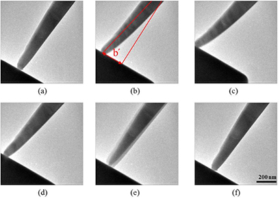
Figure 1. TEM images of deformation of Al2O3 pillar with a radius of 75 nm during a dynamic compressive process, (a)–(c) loading process; (d)–(f) unloading process.
Download figure:
Standard image High-resolution imageFigure 2 presents the TEM images of Al2O3 nanopillar of radius of 175 nm under a dynamic compression and for an unloading process. Figure 2(a) again shows the initial contact process between the pillar and diamond punch, whereas figure 2(b) displays the internal local elastic deformation of concentrated wave slowly propagating along the longitudinal direction of the pillar top at the compressive distance of 150 nm. The TEM image of pillar at a maximum compressive displacement of 180 nm given in figure 2(c) confirmed an existence of a sliding phenomenon of the nanopillar on carbon needle. Compressed pillar at beginning of the unloading process at displacement of 179 nm is shown in figure 2(d). Figure 2(e) presents TEM image taken at the unloading displacements of 28 nm. As visible from figure 2(e), during an unloading process the nanopillar was relaxed but due to a presence of the resulting internal stresses the small slip of 52 nm denoted by e' in figure 2(e) was observed.
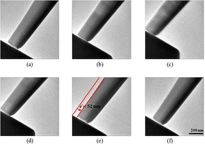
Figure 2. TEM images of deformation of Al2O3 pillar with a radius of 175 nm during a dynamic compressive process, (a)–(c) loading process; (d)–(f) unloading process.
Download figure:
Standard image High-resolution imageFigure 3 presents the normal force–displacement curve of Al2O3 pillars with radiuses of 75 and 175 nm under loading and unloading process during a dynamic compression. The maximum force occurs at load of 122.2 (160.6) µN for Al2O3 pillar with radius of 75 (175) nm, as denoted in figure 3 by a circle. Then after the maximum compressive load has been reached, the pillar was relaxed and retracted during the unloading process. The force–displacement curve reveals that the elastic deformation dominates the unloading process. We have found that the elastic energy increases with an increase of the nanopillar radius. For instance, the elastic energy of 75 nm and 175 nm thick Al2O3 nanopillars calculated based on the basis of cover area below the unloading curve are approximately 85.98 × 10⁻¹² J and 102.89 × 10⁻¹² J, respectively. Similarly, the strain energy are found to be 64.68 × 10⁻¹² J for nanopillar of radius of 75 nm and 71.08 × 10⁻¹² J for 175 nm thick pillar. Since the local contact deformations are caused by an increase of the interaction between defects during compression, therefore the contact stress induces the internal structural deformation, which contains the grain boundaries and dislocation defects.
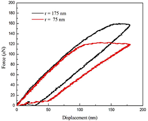
Figure 3. The normal force–displacement curve of the Al2O3 nanopillars of radii 75 and 175 nm under compression.
Download figure:
Standard image High-resolution image3.2. Stress–displacement curves of Al2O3 nanopillars during in situ TEM compression
To begin we recall a known fact that the FIB ions impacted on the Al2O3 nanopillars surface cause not only the removal of material surface but also the formation of a damaged surface with thickness of up to several nanometers, i.e. they can form an amorphous surface layer [23, 24]. Importantly, thickness of the amorphous surface layer formed on Al2O3 nanopillars surface is roughly proportional to the primary energy of Ga ions. Figure 4 displays the stress–displacement curves of Al2O3 nanopillars with radii of 75 and 175 nm during the compressive loading. In this case stress is defined as the average force F (µN) per unit area A (nm2). It is a well-known fact that the elastic limit point and macroscopic yield point (MYP) are two key points of the stress–displacement curves. The elastic limit of force per unit area of the material can arise before the onset of permanent deformation [24].
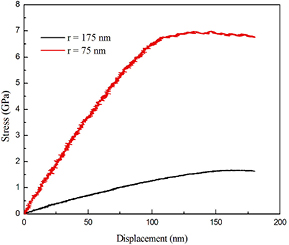
Figure 4. The stress–displacement curve of Al2O3 nanopillars with radii of 75 and 175 nm during dynamic compressive test.
Download figure:
Standard image High-resolution imageWe must emphasis here that in present work the Young's modulus of Al2O3 nanopillars were determined from results of the in situ TEM compression experiments, which are in principle different from the nanoindentation. As a result, the Young's modulus of Al2O3 nanopillar was calculated using the Euler's buckling formula [25, 26]

where E is the Young's modulus, Pcr is the critical load, L is the effective length, i.e. in our case the nanopillar effective length is 5 µm, and r0 and rL are the diameters of pillar A and B, respectively; Pcr is critical load predicted by the Rayleigh–Ritz method as Pcr = 6EI/L2. Then accounting for equation (1) and results of the compressive test the desired value of Al2O3 nanopillars Young's modulus can be easily obtained, and it reads 347.5 GPa for radius of 75 nm and 54.8 GPa for 175 nm thick pillar. The following important conclusions can be made from the in situ TEM experiments: (i) the Young's modulus decreases with an increase of the nanopillar radius; and (ii) the size and tapering effects have dominant impact on deformation of the pillar.
3.3. Mechanical properties of Al2O3 substrate obtained from nanoindentation
Here, the mechanical properties of nanopillars are determined from the nanoindentation experiments. The representative load–displacement (P–h) curves of the Al2O3 structures during nanoindentation are presented in figure 5. The hardness and the Young's modulus of prepared samples were obtained by means of the well-known quasi-static indentation method [27, 28]. The contact area A was calculated from the contact depth hc using a pre-calibrated shape function A = f(hc) of Berkovich indenter, where hc can be obtained from

where hmax is the maximum indenter penetration depth, ε is a constant, which for Berkovich indenter tip is 0.72, S is the contact stiffness during unloading and Pmax is the maximum indentation load. The Young's modulus was estimated from the following expression [29, 30]
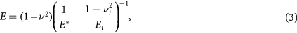
where ν and E are the Poisson's ratio and the Young's modulus, respectively; and the indenter properties were Ei = 1.14 TPa and νi = 0.07. Then E* is the effective Young's modulus given by

where S is tested sample stiffness obtained from the initial unloading slope by evaluating the maximum load and the maximum depth, i.e. S = dP/dh. Then the determined Young's modulus of the Al2O3 samples was ranging from 32.42 to 136.10 GPa. Similarly, the sample hardness was calculated from the known ratio of Pmax to the projected contact area A, where Pmax is the maximum indentation load of a prescribed sharp, i.e. Berkovich tip. The obtained hardness values of Al2O3 samples were ranging from 3.19 to 20.6 GPa.
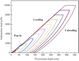
Figure 5. The representative load–displacement (P–h) curves of the Al2O3 nanopillared structures during nanoindentation at different indentation forces.
Download figure:
Standard image High-resolution imageBesides it is also evident from figure 5 that the multiple displacement discontinuities, i.e. pop-in events, were occurred during loading in ranges of 1.5–2 mN. It is worth noting that these findings are in a good agreement with the already published results [5, 31].
3.4. Mechanical properties of Al2O3 substrate obtained by the Vicker micro-hardness
An optical image of an indented Al2O3 substrate, where a square-pyramidal residual indentation remained after the Vickers test, is presented in figure 6. The Vicker hardness test is commonly used to evaluate the residual plastic behavior of solid substrates. The Vickers hardness function HV can be calculated from the load P divided by the residual surface area of indenter d in the following way

where P is load (in kg) and d is the average length of two residual indentation diagonals (in mm). It has been found that the Vickers micro-hardness of Al2O3 samples is ranging from 14 to 20.21 GPa under a loading force of 0.25–1.96 N. For readers' convenience, a comparison of the here calculated and previously reported values of Al2O3 substrate hardness H and the Young's modulus E are summarized in the table 1. As can be seen from table 1 here presented results are in a good agreement with those determined in previous studies [31–34]. Our findings confirmed that the Al2O3 substrate has a very high compression strength, high mechanical strength and extraordinary high hardness. Before the measurement, the Al2O3 substrate need to do the cutting and paste. Therefore, after the measurement of nanoindentation, the measured hardness value between this paper and previous studies may not be in a very good agreement.

Figure 6. An optical image of a Vickers hardness indent on the Al2O3 substrate after an indentation load of 1.96 N.
Download figure:
Standard image High-resolution imageTable 1. Measured mechanical properties of Al2O3 substrate and micro-structures.
| Method | Young's modulus (GPa) | Shear strength (GPa) | Hardness (GPa) | Note |
|---|---|---|---|---|
| Vickers hardness | — | — | 14.00–20.21 | Present study |
| Nanoindentation | 32.42–136.10 | — | 3.19–20.60 | Present study |
| In situ TEM | 25.52–347.5 | — | — | Present study |
| Nanoindentation | 482 ± 5 | — | 29.1 ± 0.1 | [31] |
| Nanoindentation | — | 28 ± 2 | 30 ± 3 | [32] |
| Vickers hardness | — | — | 16.2 ± 0.5 | [33] |
| Vickers hardness | — | — | 14.3–21.3 | [34] |
3.5. Raman spectrum of Al2O3 substrate
Figure 7 displays a comparative micro-Raman spectrum of Al2O3 substrate for both no indentation and indentation tests, respectively. Results given in figure 7 revealed that the Raman spectral peak of Al2O3 substrate, which did not undergo the indentation test, is similar with the one obtained previously by Li et al [35]. However, after the indentation test the peak wavenumber of Raman spectra has a production peak at 577.3 (cm−1), i.e. between 418.3 and 645.2 (cm−1) peaks. It indicates that after the indentation test of Al2O3 substrate, not only the surface was deformed but also the internal structural characteristics were changed.
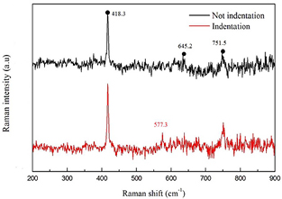
Figure 7. A comparison of the micro-Raman spectrum of Al2O3 substrate before and after indentation.
Download figure:
Standard image High-resolution image3.6. FIB micrographs of Al2O3 substrate after the Vickers hardness measurement
Figure 8 displays the FIB micrographs of Al2O3 substrate after the Vickers punched substrate by a force of 1.96 N. As it was expected a square-pyramidal residual indentation remained after the Vickers test. Figure 8(b) presents a details of the impression that was marked first in order to obtain a cross-section right thought the middle of the indent. Afterwards a platinum layer with thickness of about 1 µm was deposited on the sample surface to minimize the damage caused by the ion beam.
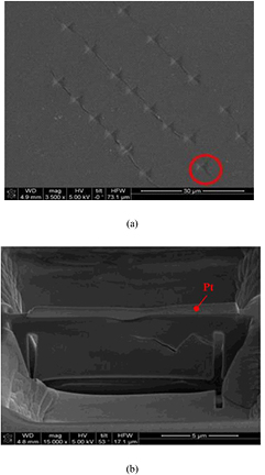
Figure 8. FIB micrographs of Al2O3 substrate after Vickers hardness indent by a force of 1.96 N, (a) SEM image after the Vickers hardness test, (b) SEM image of Al2O3 substrate is cutting by FIB (red circle in (a)).
Download figure:
Standard image High-resolution image3.7. HR-TEM micrographs of Al2O3 substrate after Vickers hardness
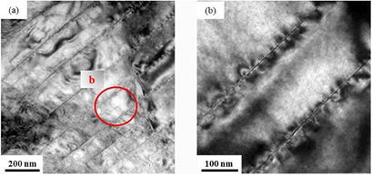
In this section, the HR-TEM images of the Al2O3 substrate after the Vickers hardness indent force of 1.96 N placed on the nickel grid right after cut embossing position by the FIB are given and the observed results are discussed in details. The HR-TEM image of Al2O3 substrate after Vickers indent, where the indent surface caused a dislocation slip line, is given in figure 9(a). This dislocation slip line was the difference in thickness direction through the film came in the TEM image of a typical form. The magnified dislocation loop shape marked by a red circle in figure 9(a) is presented in figure 9(b). As can be seen, the dislocation loop is evenly distributed alongside dislocation slip line. Consequently, it can be concluded that after the Vickers indentation of Al2O3 substrate the interior materials produced both: dislocation slip in a direction of 45° and the dislocation loop phenomenon.
Figure 9. The HR-TEM images of the Al2O3 substrate before and after the Vickers hardness indent by force of 1.96 N; (a) and (b) are images of Al2O3 substrate with created dislocation slip lines and crack deflections after the Vickers hardness indent by a load of 1.96 N; (b) is the magnified dislocation loop marked as a red cirle in image (a).
Download figure:
Standard image High-resolution image
4. Conclusion
In this study, the mechanical properties and deformation mechanism of Al2O3 nanopillars and microstructures were determined using in situ transmission electron microscopy compression and nanoindentation measurements. The obtained HR-TEM images revealed that the Al2O3 substrate contains the dislocation loops and the dislocation slip lines after the Vickers indent. After the Vicker indentation test of the Al2O3 substrate, the peak wavenumber of Raman spectra were shifted and had a production peak (577.3 cm−1) between 418.3 and 645.2 (cm−1) peak. The Young's modulus of Al2O3 nanopillars decreases with an increase of pillar diameter and in the limiting cases the Young's modulus of Al2O3 were 347.5 GPa for pillar of radius of 75 nm and 54.8 GPa for the one of radius of 175 nm. Overall, here presented results provide the key fundamental information required for better understanding of the mechanical properties, contact behavior and local bending of Al2O3 micro- and nanostructures including nanopillars.
Acknowledgments
This work was supported by the Ministry of Science and Technology of Taiwan under grants MOST 103-2221-E-151-001-MY3 and MOST 103-2221-E-151-007-MY3.